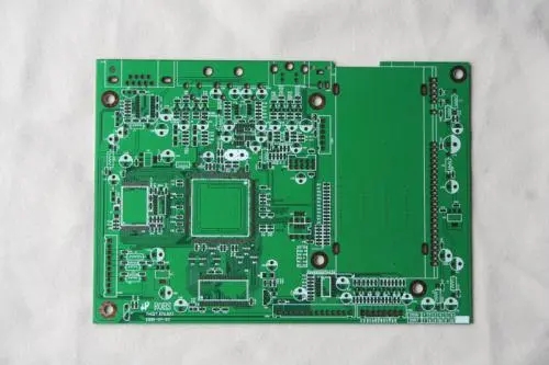
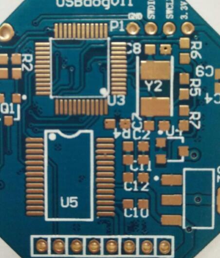
PCB proofing has always been, the main concern of the test engineer is to ensure that he has an effective test program, the program can be well executed in production. "In-Circuit Test (ICT)" is still a very effective method of detecting manufacturing defects. More advanced ICT systems can also add actual value to the test function configuration by providing methods for programming Flash memory, PLD, FPGA and EEPROM during testing. The Agilent 3070 system is the market leader in ICT.
Now ICT still plays an important role in the PCB manufacturing and testing process of printed circuit board assembly(PCA), but what impact will people's pursuit of lead-free PCB have on the ICT stage?

The promotion of lead-free soldering technology has led to a lot of research on PCB surface treatment technology. These studies are mainly based on the technical performance in the PCB construction process. The influence of different PCB surface treatment technologies on the testing stage is mostly ignored, or only focus on contact resistance. This report will introduce the details of the effects observed in ICT and the need to respond to and understand these changes.
PCB proofing surface treatment experience, and training engineers for the realization of ICT PCB production process changes. This article will talk about the surface treatment of lead-free PCB, especially in the ICT stage of the manufacturing process, and reveal that the successful test of lead-free surface treatment also depends on the beneficial contribution of the PCB construction process.
A successful ICT test is always related to the physical characteristics of the contact points between the test probes of the needle bed fixture and the test pads on the PCB. When a very sharp probe touches a soldered test point, the solder will dent because the contact pressure of the probe is much higher than the yield strength of the solder. As the solder dents, the probe penetrates any impurities on the surface of the test pad. The uncontaminated solder below is now in contact with the probe to achieve good contact with the test point. The depth of probe insertion is a direct function of the yield strength of the target material. The deeper the probe penetrates, the better the contact.
An 8-ounce (oz) probe can apply a contact pressure of 26,000 to 160,000 psi (pounds per square inch), depending on the surface diameter. Because the yield strength of solder is about 5,000 psi, the contact of the probe is better for this relatively soft solder.
PCB proofing surface treatment process selection
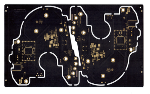
Before we understand the cause and effect, it is very important to describe the types of PCB surface treatment processes available and what these types can provide. All printed circuit boards (PCBs) have a copper layer on the board. If the copper layer is not protected, it will be oxidized and damaged. There are many different protective layers available, the most common ones are hot air solder leveling (HASL), organic solder protection (OSP), electroless nickel-gold immersion (ENIG), silver immersion, and tin immersion.
Hot air solder leveling (HASL)
PCB proofing HASL is the main leaded surface treatment process used in the industry. The process is formed by immersing the circuit board in a lead-tin alloy, and the excess solder is removed by an "air knife". The so-called air knife is hot air blowing on the surface of the board. For the PCA process, HASL has many advantages: it is the cheapest PCB, and the surface layer can be soldered after multiple reflow soldering, cleaning and storage. For ICT, HASL also provides a process for automatically covering test pads and vias with solder. However, compared with the existing alternative methods, the flatness or coplanarity of the HASL surface is poor. Now there are some lead-free HASL alternative processes, which are becoming more and more popular due to the natural replacement characteristics of HASL. For many years, HASL has been applied with good results, but with the emergence of "environmentally friendly" green process requirements, the existence of this process is numbered. In addition to the lead-free problem, increasing board complexity and finer pitch have exposed many limitations of the HASL process.
Advantages: PCB proofing surface technology, maintains solderability throughout the manufacturing process, and has no negative impact on ICT.
Disadvantages: Usually lead-containing processes are used. Lead-containing processes are now restricted and will eventually be eliminated by 2007. For fine pin pitch (<0.64mm), it may cause solder bridging and thickness problems. The uneven surface can cause coplanarity problems in the assembly process.
PCB proofing organic solder protector
Organic Solder Protector (OSP) is used to produce a thin, uniform protective layer on the copper surface of the PCB. This coating protects the circuit from oxidation during storage and assembly operations. This process has been around for a long time, but only recently has it gained popularity as lead-free technology and fine-pitch solutions are sought.
In terms of coplanarity and solderability, OSP has better performance in PCA assembly than HASL, but requires significant process changes to the type of flux and the number of thermal cycles. Because of its acidic characteristics will reduce OSP performance and make copper easy to oxidize, so careful handling is required. Assemblers prefer to treat metal surfaces that are more flexible and can withstand more thermal cycles.
The surface treatment of the OSP of the PCB proofing, if the test point is not welded, will cause the contact problem of the needle bed fixture in the ICT. Merely changing to a sharper probe type to penetrate the OSP layer will only cause damage and puncture the PCA test via or test pad. Studies have shown that switching to a higher detection force or changing the probe type has little effect on yield. Untreated copper has an order of magnitude higher yield strength than leaded solder, and the only result is that it will damage the exposed copper test pad. All testability guidelines strongly recommend not to directly probe exposed copper. When using OSP, it is necessary to define a set of OSP rules for the ICT phase. The most important rule requires that the Stencil be opened at the beginning of the PCB process to allow solder paste to be applied to the test pads and vias that need to be contacted by the ICT.
Advantages: Comparable with HASL in unit cost, good coplanarity, lead-free process, and improved solderability.
Disadvantages: The assembly process needs to undergo major changes. If the unprocessed copper surface is detected, it will be detrimental to ICT. Over-pointed ICT probes may damage the PCB, requiring manual precautions, limiting ICT testing and reducing test repeatability.
PCB proofing electroless nickel-gold immersion
Electroless nickel-gold immersion (ENIG) coating has been successfully applied on many circuit boards. Although it has a higher unit cost, it has a flat surface and excellent solderability. The main disadvantage is that the electroless nickel layer is very fragile and has been found to be broken under mechanical pressure. This is called "black block" or "mud crack" in the industry, which has led to some negative reports from ENIG.
Advantages: good solderability, flat surface, long storage life, can withstand multiple reflow soldering.
Disadvantages: high cost (about 5 times of HASL), "black block" problem, manufacturing process using cyanide and other harmful chemicals.
PCB proofing silver immersion
Silver immersion is a newly added method of PCB surface treatment. It is mainly used in Asia and is being promoted in North America and Europe.
During the soldering process, the silver layer melts into the solder joints, leaving a tin/lead/silver alloy on the copper layer. This alloy provides a very reliable solder joint for BGA packages. Its contrasting color makes it easy to be inspected, and it is also a natural alternative to HASL in welding.
Silver immersion is a surface processing technology with very promising development prospects, but like all new surface processing technologies, end users are very conservative. Many manufacturers regard this process as a "under investigation" process, but it is likely to become the best lead-free surface process choice.