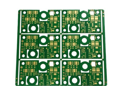
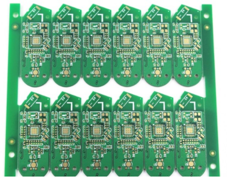
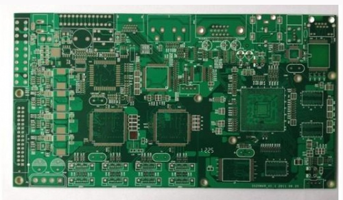
Although the current EDA tools are very powerful for PCB proofing, as the PCB size requirements are getting smaller and smaller, the device density is getting higher and higher, and the difficulty of PCB design is not small. How to achieve a high PCB layout rate and shorten the design time? This article introduces the design skills and key points of PCB planning, layout and wiring. Now PCB design time is getting shorter and shorter, smaller and smaller circuit board space, higher and higher device density, extremely demanding layout rules and large-size components make the designer's work more difficult. In order to solve the design difficulties and speed up the launch of products, many PCB manufacturers now tend to use dedicated EDA tools to realize PCB design. However, dedicated EDA tools cannot produce ideal results, nor can they achieve a 100% deployment rate, and are very messy. It usually takes a lot of time to complete the remaining work.

There are many popular EDA tool software on the market, but they are all the same except for the different terminology used and the position of the function keys. How to use these tools to better realize the PCB design? A careful analysis of the design and careful settings of the tool software before starting the wiring will make the design more in line with the requirements. The following is the general design process and steps.
1, PCB proofing to determine the number of layers of the PCB
The size of the circuit board and the number of wiring layers need to be determined at the beginning of the design. If the design requires the use of high-density ball grid array (BGA) components, the minimum number of wiring layers required for wiring these devices must be considered. The number of wiring layers and the stack-up method will directly affect the wiring and impedance of the printed lines. The size of the board helps determine the stacking method and the width of the printed line to achieve the desired design effect.
For many years, people have always believed that the lower the number of layers of the circuit board, the lower the cost, but there are many other factors that affect the manufacturing cost of the circuit board. In recent years, the cost difference between multilayer boards has been greatly reduced. It is best to use more circuit layers and evenly distribute the copper at the beginning of the design, so as to avoid discovering that a small number of signals do not meet the defined rules and space requirements until the end of the design, so that new layers are forced to be added. Careful planning before designing will reduce a lot of troubles in wiring.
2, PCB proofing design rules and restrictions
The automatic routing tool itself does not know what to do. In order to complete the wiring task, the wiring tool needs to work under the correct rules and restrictions. Different signal lines have different wiring requirements. All signal lines with special requirements must be classified, and different design classifications are different. Each signal class should have a priority, the higher the priority, the stricter the rules. The rules involve the width of the printed lines, the maximum number of vias, the degree of parallelism, the mutual influence between the signal lines, and the limitation of layers. These rules have a great influence on the performance of the wiring tool. Careful consideration of design requirements is an important step for successful wiring.
3, the layout of PCB proofing components
In order to optimize the assembly process, design for manufacturability (DFM) rules will restrict component layout. If the assembly department allows the components to move, the circuit can be appropriately optimized, which is more convenient for automatic wiring. The defined rules and constraints will affect the layout design.
The routing channel and via area need to be considered during layout. These paths and areas are obvious to the designer, but the automatic routing tool will only consider one signal at a time. By setting routing constraints and setting the layer of the signal line, the routing tool can be as the designer imagined Complete the wiring like that.
4, PCB proofing fan-out design
In the fan-out design stage, to enable automatic routing tools to connect component pins, each pin of the surface mount device should have at least one via, so that when more connections are needed, the circuit board can be internally layered Connection, online testing (ICT) and circuit reprocessing.
In order to maximize the efficiency of the automatic routing tool, the largest via size and printed line must be used as much as possible, and the interval is set to 50mil. Use the via type that maximizes the number of routing paths. When carrying out fan-out design, it is necessary to consider the problem of circuit online testing. Test fixtures can be expensive, and they are usually ordered when they are about to go into full production. If only then consider adding nodes to achieve 100% testability, it would be too late.
After careful consideration and prediction, the design of circuit online test can be carried out at the early stage of the design and realized in the later stage of the production process. The type of via fan-out is determined according to the wiring path and circuit online test. The power supply and grounding will also affect the wiring and fan-out design. . In order to reduce the inductive reactance generated by the connection line of the filter capacitor, the vias should be as close as possible to the pins of the surface mount device, and manual wiring can be used if necessary. This may affect the originally envisaged wiring path, and may even cause you to re- Consider which type of via to use, so the relationship between via and pin inductance must be considered and the priority of via specifications must be set.
5, PCB proofing manual wiring and key signal processing
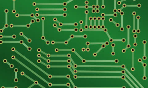
Although this article mainly discusses automatic wiring problems, manual wiring is an important process of printed circuit board design now and in the future. The use of manual wiring helps automatic wiring tools to complete the wiring work. As shown in Figure 2a and Figure 2b, by manually routing and fixing the selected nets, a path that can be followed during automatic routing can be formed.
Regardless of the number of key signals, these signals should be routed first, either manually or in combination with automatic routing tools. Critical signals usually have to pass careful circuit design to achieve the desired performance. After the wiring is completed, the relevant engineering personnel will check the signal wiring. This process is relatively easy. After passing the inspection, fix these lines, and then start to automatically route the remaining signals.
6, automatic wiring
The wiring of key signals needs to consider controlling some electrical parameters during wiring, such as reducing distributed inductance and EMC, etc. The wiring of other signals is similar. All EDA vendors will provide a way to control these parameters. After understanding the input parameters of the automatic wiring tool and the influence of the input parameters on the wiring, the quality of the automatic wiring can be guaranteed to a certain extent.
General rules should be used to automatically route signals. By setting restrictions and prohibiting wiring areas to limit the layers used by a given signal and the number of vias used, the wiring tool can automatically route the wires according to the engineer's design ideas. If the number of layers used by the automatic routing tool and the number of vias are not limited, each layer will be used during automatic routing, and many vias will be generated.
After setting the constraints and applying the created rules, the automatic routing will achieve similar results as expected. Of course, some sorting work may be required, and space for other signals and network wiring needs to be ensured. After a part of the design is completed, fix it to prevent it from being affected by the subsequent wiring process.
Use the same steps to route the remaining signals. The number of wiring depends on the complexity of the circuit and the number of general rules you define. After each type of signal is completed, the constraints of the remaining network wiring will be reduced. But what comes with it is that a lot of signal wiring requires manual intervention. Today's automatic wiring tools are very powerful and can usually complete 100% of the wiring. However, when the automatic wiring tool has not completed all signal wiring, the remaining signals need to be manually wired.
7, the main points of the design of PCB proofing automatic wiring include:
7.1 Change the settings slightly, try a variety of route wiring;
7.2 Keep the basic rules unchanged, try different wiring layers, different printed lines and spacing widths, different line widths, and different types of vias such as blind vias, buried vias, etc., and observe how these factors affect the design results;
7.3 Let the wiring tool handle those default networks as needed;
7.4 The less important the signal is, the more freedom the automatic routing tool has for its routing.
8, PCB proofing wiring arrangement
If the EDA tool software you are using can list the signal wiring length, check these data, you may find that some signal wiring lengths with few constraints are very long. This problem is relatively easy to deal with, and the signal wiring length can be shortened and the number of vias can be reduced by manual editing. In the finishing process, you need to determine which wiring is reasonable and which wiring is unreasonable. Like manual wiring design, automatic wiring design can also be sorted and edited during the inspection process.
9, the appearance of the PCB proofing circuit board
The previous design often paid attention to the visual effect of the circuit board, but now it is different. The automatically designed circuit board is not as beautiful as the manual design, but the electronic characteristics can meet the specified requirements, and the complete performance of the design is guaranteed.