We want to make an electronic product for PCB proofing, usually by designing the schematic circuit diagram first. On the circuit schematic diagram, various specific symbols are used to represent different electronic components and connect them with wires. An electronic engineer can pass These symbols and connections clearly show the working principle of the circuit and the function of each part. If the circuit design is correct, you only need to prepare the required electronic components, and then connect them with wires to work. Most of the electronic products are like this.If you still have a tube radio from the 1960s and 1970s at home, you can see those messy components and criss-cross wires.

Fortunately, the circuit of the tube radio is relatively simple, but if you want to make a more complicated product, such as a computer motherboard, you can think about it, if you still use the above method to do it, what will be the result. That may be necessary Tens of thousands of wires are soldered one by one. I am afraid that the most skilled workers will also get tired. In addition, mass production cannot be carried out with this method. Therefore, we need PCB.
What is PCB
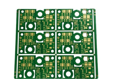
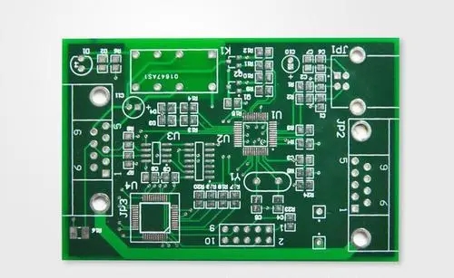
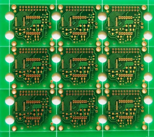
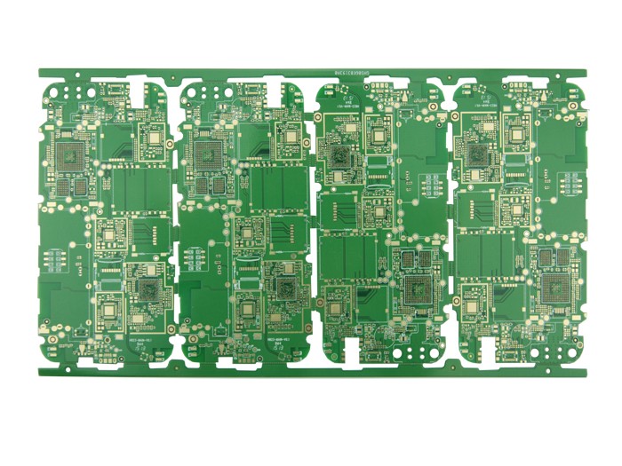
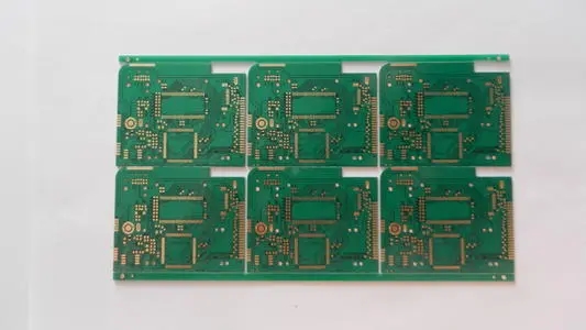
PCB is the abbreviation of "Printed Circuit Board" in English. The literal translation is the meaning of printed circuit board. Its meaning is: a board of a certain size is processed with an insulating material as a substrate, and there is at least one conductive pattern and a designed hole on it. Realize the electrical connection between electronic components, such a board is called a printed circuit board.
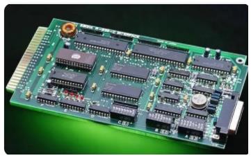
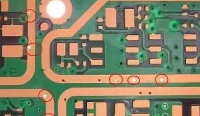
PCB proofing Generally speaking, the PCB is obtained by etching a copper-clad board. The copper-clad board is composed of a board base and copper foil. The board base is usually made of insulating materials such as glass fiber and covered with a layer of copper foil (usually oxygen-free copper). After the copper foil is etched, there is a section of zigzag copper foil. These copper foils are called traces. The functions of these traces are equivalent to those in the circuit schematic diagram. They are responsible for connecting the components The pins are connected together. There are some holes drilled in the copper foil for mounting electronic components, called drilling. The copper foil used for soldering with the component pins is called a pad (Pad).
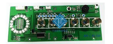
Obviously, PCB can provide fixed and assembled mechanical support for electronic components, and can realize electrical connection or insulation between electronic components. In addition, we can also see that many PCBs are printed with component numbers and some graphics. This It provides convenience for component insertion, inspection and maintenance.
How can components be mounted on the PCB
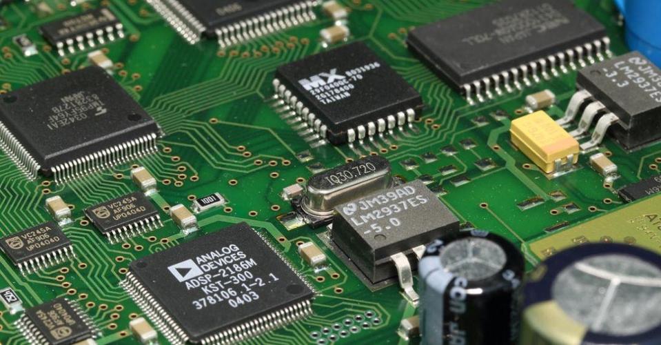
Since we have talked about the PCB's ability to provide mechanical support and electrical connections for electronic components, how do these electronic components be mounted on the PCB? In fact, there are many types of packaging for electronic components, and components of different packaging forms are in The mounting method on the PCB is also different. Traditional electronic components are mostly pin-type and larger in size. For this kind of components, they need to be drilled on the PCB before they can be installed. The component pins pass through the holes and are soldered to the PCB. On the other side of the pad, the excess pins must be cut after the soldering is completed. But now computer boards are more low-cost and small-sized SMD surface mount components, so there is no need to drill holes on the PCB, just stick In the designed position, solder the component on the pad. In addition to the component can be directly soldered on the PCB, it can also be installed through a socket. For example, most of the well-known BIOS chips are installed on the motherboard with a socket. .
The concept of component surface and soldering surface is often mentioned in some materials. The so-called component surface is the surface where the electronic component is located. The soldering surface is the surface where the pins of the component are connected to the pads on the PCB through soldering. It is our For soldering. For pin-type components, the solder joints and components are on the two sides of the PCB, and the components can only be on the component side, otherwise it will bring huge trouble to soldering. For SMD components, solder joints and components They are all on one side, so the components can be on any one or even two sides of the PCB.