In general, when the signal interconnection delay is greater than 20% of the edge signal flipping threshold time, the signal wires on the board will show the transmission line effect, that is, the connection is no longer a simple wire that displays lumped parameters. Performance, but showing the effect of distributed parameters, this design is a high-speed design. In the design of high-speed digital systems, designers must solve the problem of false flipping and signal distortion caused by parasitic parameters-that is, timing and signal integrity issues. At present, this is also a bottleneck problem that high-speed circuit designersmust solve.

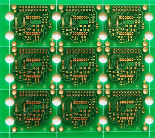
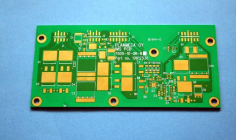
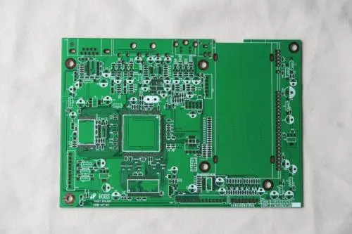
PCB proofing is driven by traditional physical rules
We can find that in traditional high-speed circuit design, electrical rule setting and physical rule setting are separate. This brings the following shortcomings:
In the early stages of design, engineers had to spend a lot of energy on detailed front-end and back-end (that is, logical establishment-physical realization) analysis to plan a physical wiring strategy that meets electrical requirements.
The high-speed effect is a complicated subject, and the expected effect cannot be achieved simply by controlling the wiring length and parallel lines.
The designer will inevitably face such a dilemma. The physical rules with false components are not applicable in actual wiring. He has to modify the rules repeatedly to make them have practical value.
When the wiring is completed, the post-verification tool can be used for analysis. But if a problem is found, the engineer must return to the design and adjust the structure or rules. This is a cyclic redundant process. It will inevitably affect the time to market.
When there are only a few or dozens of critical wire nets in the design, the physical rule drive can complete the design task well; but when there are hundreds or even thousands of wire nets in the design, the physical rule-driven method is fundamental Inability to perform design tasks. The development of electronic technology calls for the emergence of new methods and tools to solve the bottleneck problems faced by the design. In order to solve the shortcomings of physical rule-driven high-speed design, people of insight in the industry engaged in the development of high-speed digital circuit design EDA tools proposed the concept of real-time electrical rules-driven physical layout three years ago. Reforms were carried out.
A new electrical rule-driven for PCB proofing: interconnection synthesis
Interconnection synthesis is a typical term for the real-time electrical rule-driven method. That is, in the physical layout and routing process, the interconnection synthesizer performs real-time analysis according to the constraints of the electrical rules, and extracts the wiring strategy that meets the designer's requirements, so that the design is successful in one pass. This method accurately integrates electrical requirements and physical realization through interconnection and synthesis, and fundamentally eliminates the defects of the physical rule-driven method.
The integrated process of PCB proofing interconnection is as follows:
Input noise constraints and timing constraints rules in the tool;
Timing control layout to meet timing constraint requirements;
Perform signal integrity pre-optimization;
Board-level integration to ensure that the critical line network meets electrical requirements;
Complete the wiring of ordinary wire netting;
Comprehensive optimization of wiring.
The electrical rule-driven method can effectively evaluate the quality before designing the layout, detect the signal distortion, and determine the matching network topology and the appropriate terminal matching structure and resistance. After the layout is completed, post-verification can be performed, and the waveform can be inspected intuitively with a software oscilloscope. The timing and distortion problems found at this time can be solved by the routing synthesis optimization function.
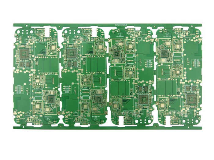
PCB Proofing Gold Tool Combination and Design Process
Now many EDA manufacturers can provide EDA tools for high-speed system PCB design to help users effectively improve design quality and shorten design cycles in this field. The most representative of the EDA system board-level tools that apply the electrical rule-driven method is the ICX software package from MentorGraphics of the United States. It was the first to propose the concept of interconnection and synthesis, and it is also the most mature tool combination in the industry. This software package has the current industry-popular plug-and-play feature, and it can be integrated into the PCB classic EDA design process of many manufacturers.