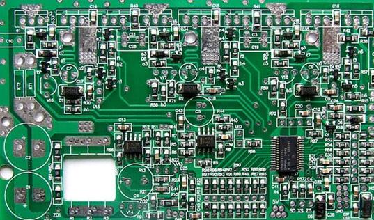
Factors affecting the quality of exposure imaging by circuit board factories

(1) Selection of light source
In the PCB factory, any dry film has its own unique spectral absorption curve, and any light source also has its own emission spectrum curve. If the main spectral absorption peak of a certain dry film overlaps or overlaps most of the main spectral emission peak of a certain light source, the two match well and the exposure effect is the best. The spectral absorption curve of the domestic dry film shows that the spectral absorption region is 310 ~ 440nm. Dy lamp, high pressure mercury lamp, and iodine gallium lamp have relatively large relative radiation intensity in the wavelength range of 310 ~ 440nnl, which is an ideal light source for dry film exposure. .
(2) Control of exposure time
In the light-gathering process, the photopolymerization reaction of the dry film does not complete the reaction at the sight of light, but requires a certain exposure time
Carry out an adequate response:
When the exposure is insufficient, due to the incomplete polymerization of the monomer, the film swells and becomes soft during the development process, and the lines are not clear.
The color is dim, or even stale. During the pre-treatment of electroplating or the process of electric quilting, the film is warped, infiltrated, or even peeled off;
In the circuit board factory, it will be difficult to develop, the film will be brittle, and the residual glue will be left. Incorrect exposure will cause deviation of image line width, and excessive exposure will cause pattern plating The thinning of the lines makes the printed and etched lines thicker. On the contrary, insufficient exposure makes the lines of the pattern plating thicker, and the printed and etched lines become thinner. In order to determine the exposure time, it is usually recommended to use a Riston 17-level or Sbuffer 21-level optical densitometer.
Factors that affect the quality of exposure and imaging of circuit board factories
The circuit board factory also needs to pay attention to the visual positioning in the exposure positioning:
The visual positioning of the circuit board factory is usually suitable for the use of a diazo master. The diazo master is brown or orange in a semi-transparent state; but it is not transparent to ultraviolet light, and the pad of the master is overlapped with the hole of the printed board through the diazo image. Align and fix with tape to perform exposure.
Out of stock positioning system positioning.
The above is an introduction to the factors that affect the quality of exposure and imaging of circuit board factories. Ipcb is also provided to PCB manufacturers and PCB manufacturing technology