DIP plug-in considerations
The Internet era has broken the traditional marketing model, and a large number of resources have been gathered together to the greatest extent through the Internet, which has also accelerated the development speed of FPC flexible circuit boards, and then as the development speed accelerates, environmental problems will continue to appear in PCB factories. In front of him. However, with the development of the Internet, environmental protection and environmental informatization have also been developed by leaps and bounds. Environmental information data centers and green electronic procurement are gradually being applied to the actual production and operation fields.
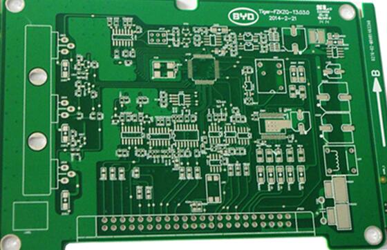
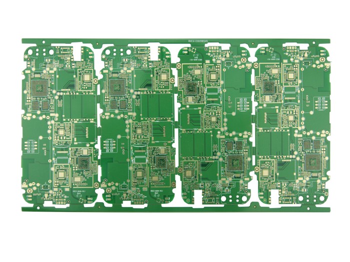
DIP plug-in post-welding processing is a process after SMT patch processing, and the processing flow is as follows:
1. Pre-process the components
The staff of the pre-processing workshop pick up the materials from the material place according to the BOM material list, carefully check the material model, specification, sign, and perform pre-production pre-processing according to the sample (using automatic bulk capacitor clipper, transistor automatic molding machine, automatic belt type Molding machines and other molding equipment for processing).
Require:

1. The horizontal width of the adjusted component pins needs to be the same as the width of the *** hole, and the tolerance is less than 5%;
2. The distance between the component pins and the PCB pads should not be too large;
3. If the customer requests, the parts need to be molded to provide mechanical support to prevent the pad from lifting.
2. Paste high-temperature adhesive paper, feed the board - paste high-temperature adhesive paper, and block the tin-plated through holes and the components that must be soldered afterwards;
3. DIP plug-in processing workers need to wear static rings, wear anti-static clothes and hats to prevent static electricity, and plug in according to the component BOM list and component bit number map. The plug-in should be carefully and carefully, and no wrong or missing plugs;
4. For the inserted components, inspections should be carried out, mainly to check whether the components are inserted incorrectly or missing;
5. For the PCB board with no problem with the plug-in, the next step is to pass the wave soldering, and use the wave soldering machine to perform the automatic soldering process, which is the solid component;
6. Remove the high-temperature adhesive tape, and then perform inspection. In this link, it is mainly a visual inspection, to observe whether the welded PCB board is well welded or not;
7. Repair welding and repairing the PCB boards that are not completely welded to prevent problems;
8. Post welding, this is a process set for specially required components, because some components cannot be directly welded by wave soldering machines according to the limitations of the process and materials, and need to be completed manually;
9. After all the components are welded, the PCB board should be tested for function to test whether each function is normal. If the function defect is found, it should be repaired and tested again.