From the perspective of signal traces, a good layering strategy should be to put all signal traces on one or several layers, and these layers are next to the power layer or ground layer. For the power supply, when the PCB multilayer circuit board is produced, a good layering strategy should be that the power layer is adjacent to the ground layer, and the distance between the power layer and the ground layer is as short as possible.

There are several potential problems with the 4-layer board design. First of all, the traditional 4-layer board with a thickness of 62 mils, even if the signal layer is on the outer layer, and the power and ground layers are on the inner layer, the distance between the power layer and the ground layer is still too large. If the cost requirement is the first, you can consider the two traditional 4-layer board alternatives listed in Table 3-7. These two schemes can improve the performance of EMI suppression, but they are only suitable for the occasions where the component density on the board is low enough and there is enough area around the components (place the required power copper layer).
The first is the preferred solution. The outer layer of the PCB is the ground layer, and the middle two layers are the signal/power layer. The power supply on the signal layer is routed with a wide wire, which can make the path impedance of the power supply current low, and the impedance of the signal path also becomes low. From the perspective of EMI control, this is the best 4-layer PCB structure available.
In the second scheme, the outer layer uses power and ground, and the middle layer uses signals. Compared with the traditional 4-layer board, this solution has a smaller improvement effect, and the interlayer impedance is as poor as the traditional 4-layer board.
If you want to control the trace impedance, in the above-mentioned stacking scheme, you must carefully arrange the traces under the power and ground copper-clad islands. In addition, the copper-clad islands on the power or ground plane should be interconnected as much as possible to ensure DC and low-frequency connectivity.
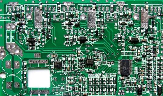
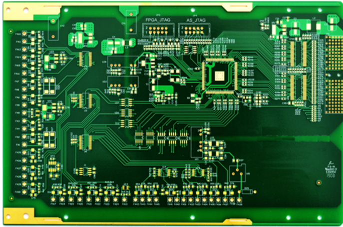
The above is the introduction to the laminated design of the four-layer board of the PCB multi-layer circuit board manufacturer. Ipcb is also provided to the PCB manufacturer and PCB manufacturing technology.