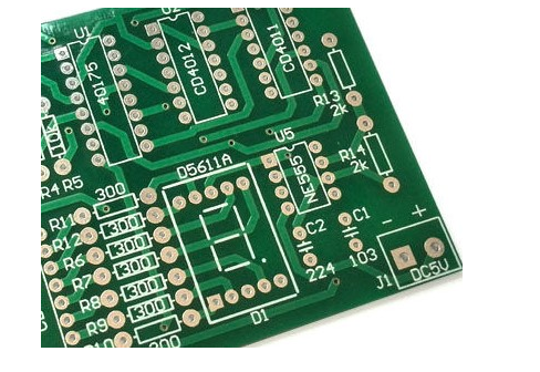
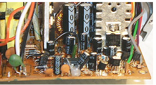
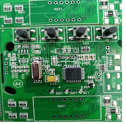
Reversal of PCB schematic
The schematic diagram is a drawing composed of electrical symbols used to analyze the principle of the circuit. It plays an indispensable role in the process of product debugging, maintenance, and improvement. The reverse design of the schematic diagram is the opposite of the forward design. The forward design is the design of the schematic first, and then the PCB design based on the schematic. The reverse design of the PCB refers to the reverse deduction of the product based on the existing PCB file or the actual PCB. Schematic diagram to facilitate the technical analysis of the product and to assist the later product prototype debugging production or improvement and upgrade.

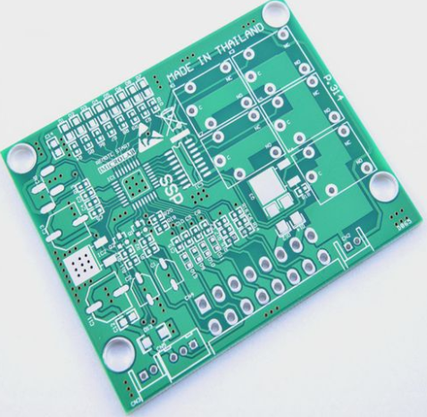
BOM list production
In the process of product reverse technology research and imitation development, the production of the BOM list and the placement map, and the production of the component coordinate map for the SMT placement machine are all necessary for later model welding, placement processing, complete prototype design and assembly production. Link.
BOM (Bill of Materials) is the basis for the purchase of device materials. It records various components, modules and other special materials required for product composition. The most important thing in the preparation of the BOM list is to require accurate measurement of various parameters of the components, because if the device parameters are wrong, it may affect the judgment of the device and the accuracy of material procurement, and may even lead to the failure of project development.
PCB change board
PCB boardmodification is a related concept in PCB copy board. It refers to the circuit adjustment or re-layout of the extracted PCB file to realize the functional modification of the original circuit board, which can quickly realize the update and upgrade of the product to satisfy some customers. Individual needs and special application requirements.
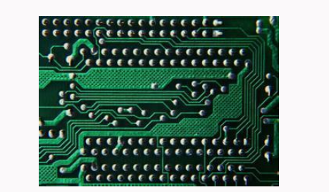
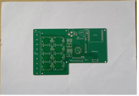
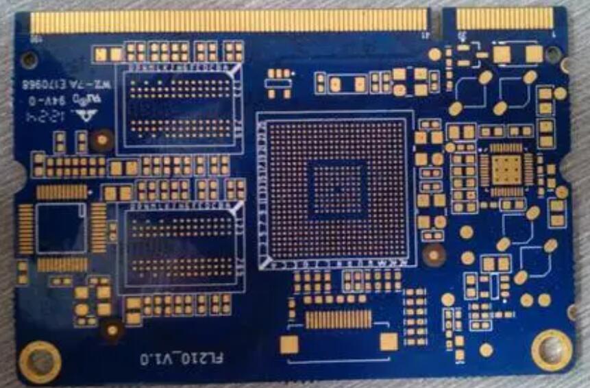
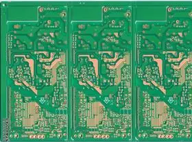
PCB design
In high-speed design, the characteristic impedance of controllable impedance boards and lines is one of the most important and common problems. First understand the definition of a transmission line: a transmission line is composed of two conductors with a certain length, one conductor is used to send signals, and the other is used to receive signals (remember the concept of "loop" instead of "ground"). In a multilayer board, each line is a component of the transmission line, and the adjacent reference plane can be used as the second line or loop. The key to a line becoming a "good performance" transmission line is to keep its characteristic impedance constant throughout the line.
The key to the circuit board becoming a "controllable impedance board" is to make the characteristic impedance of all circuits meet a specified value, usually between 25 ohms and 70 ohms. In a multilayer circuit board, the key to good transmission line performance is to keep its characteristic impedance constant throughout the line.
But what is the characteristic impedance? The easiest way to understand characteristic impedance is to look at what the signal encounters during transmission. When moving along a transmission line with the same cross-section, this is similar to the microwave transmission shown in Figure 1. Suppose a voltage step wave of 1 volt is applied to this transmission line. For example, a 1 volt battery is connected to the front end of the transmission line (it is located between the transmission line and the loop). Once connected, the voltage wave signal travels along the line at the speed of light. Propagation, its speed is usually about 6 inches/nanosecond. Of course, this signal is indeed the voltage difference between the transmission line and the loop, and it can be measured from any point of the transmission line and the adjacent point of the loop. Fig. 2 is a schematic diagram of the transmission of the voltage signal.
Zen's method is to first "generate a signal" and then propagate it along this transmission line at a speed of 6 inches per nanosecond. The first 0.01 nanosecond advances 0.06 inches. At this time, the sending line has excess positive charge, and the loop has excess negative charge. It is the difference between these two kinds of charges that maintains the 1 volt voltage difference between the two conductors. And these two conductors form a capacitor.
In the next 0.01 nanosecond, to adjust the voltage of a 0.06 inch transmission line from 0 to 1 volt, it is necessary to add some positive charge to the transmitting line and some negative charge to the receiving line. For every 0.06 inch of movement, more positive charge must be added to the transmission line, and more negative charge must be added to the loop. Every 0.01 nanoseconds, another section of the transmission line must be charged, and then the signal starts to propagate along this section. The charge comes from the battery at the front end of the transmission line. When moving along this line, it charges the continuous part of the transmission line, thus forming a voltage difference of 1 volt between the transmission line and the loop. Every 0.01 nanosecond of advancement, some charge (±Q) is obtained from the battery, and the constant amount of electricity (±Q) flowing out of the battery in a constant time interval (±t) is a constant current. The negative current flowing into the loop is actually the same as the positive current flowing out, and it is just at the front end of the signal wave. The AC current passes through the capacitor formed by the upper and lower lines to end the entire cycle.