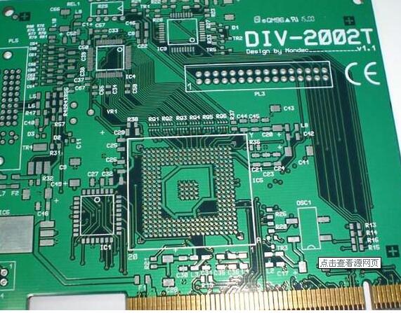
Automatic online detection in smt processing
iPCB attaches great importance to customer satisfaction, so we have established a responsible customer complaint department. If you are dissatisfied with our products after receiving our products, you can ask us to refund to your iPCB credit account, or request to re-produce the failed order. Of course, if you are still dissatisfied with our service or have any suggestions, you can send an email to us so that we can spend more time improving our services and establishing a complete suggestion system to satisfy our customers and ensure their interests.
First of all, because this equipment is an independent system, it can be tested without using the hardware of the printing press and without stopping the machine;
Secondly, the measurement performance of the testing equipment can obtain accurate and repeatable measurement results. The automatic online testing system can choose the method of sample testing, sampling testing or whole board testing according to the actual production situation.
With the advent of high-speed testing equipment and people's high-quality and high-reliability requirements for electronic products, the method of automatic on-line inspection of the entire board is mainly used to inspect the quality of solder paste printing.

The automatic online inspection of the whole board is to use a laser beam to scan the entire PCB on the SMT chip processing plant line by line, collect the measurement data of each pad solder paste printing, and compare the actual measurement value with the preset qualification limit Value to compare.
The whole board automatic online inspection equipment can detect accidental defects such as solder paste leakage caused by blockage of the template opening, as well as defects such as solder paste collapse, solder paste printing blur, dent, sharpening, solder paste bulge and offset.
The whole board automatic online inspection equipment can point out the location, defect name and hazard degree of each printing defect, and collect all the solder paste printing information on the PCBA. At present, the automatic online inspection equipment for the entire solder paste printing board mainly includes automatic optical inspection (Automatic optical inspection). Optic Inspection, AOI) system and solder paste inspection system.
1. AOI system.
The automatic optical inspection system adopts computer technology, high-speed image processing and recognition technology, etc., with automatic, high-speed and high-resolution inspection capabilities, thereby improving the objectivity and accuracy of discrimination, reducing special fixtures, and providing real-time feedback information to the production system .
In smt factory patch processing, AOI is mainly used for the inspection of 3 processes, and the inspection after solder paste printing is one of its inspection processes. Through the inspection after solder paste printing, the defects in the printing process can be found in time, and the defects caused by poor solder paste printing can be minimized.
2. SPI system.
The solder paste inspection system is formed on the basis of AOI technology, and there are two main measurement methods:
One is to use laser triangulation technology.
The second is a measurement technology based on Moire technology.
The laser triangulation technique is combined with two-dimensional images to determine the difference between the measured target height and the standard height. The main disadvantages are low accuracy and insufficient resolution. Because the laser triangulation technique has only one light source, it cannot accurately calculate the volume of solder paste. At present, the country has higher and higher requirements for environmental protection and greater efforts in link governance. This is a challenge but also an opportunity for PCB factories. If the PCB factory is determined to solve the problem of environmental pollution, then FPC flexible circuit board products can be at the forefront of the market, and the PCB factory can get the opportunity to develop again.