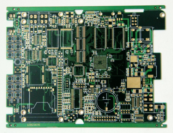
Sort out the advantages and disadvantages of several common PCB surface treatments
With the evolution of the times, the advancement of science and technology, and the requirements of environmental protection, the electronics industry is also actively or forcedly advancing along with the great wheels of the times, so why not the technology of circuit boards. The surface treatment of several kinds of circuit boards is currently the more common process. I can only say that there is no perfect surface treatment at present, so there are so many choices. Each surface treatment has its own advantages and disadvantages. Next interview To enumerate:
Bare copper plate:
Advantages: low cost, smooth surface, good weldability (in the absence of oxidation).
Deficiency: It is easily affected by acid and humidity and cannot be stored for a long time. It must be used up within 2 hours after unpacking, because copper is easily oxidized when exposed to the air; it cannot be used in the double-sided process because the first reflow soldering process The two sides are already oxidized. If there is a test point, solder paste must be printed to prevent oxidation, otherwise it will not be in good contact with the probe.

Spray tin plate (HASL, Hot Air Solder Levelling, hot air solder leveling):
Advantages: better Wetting effect can be obtained, because the plating layer itself is tin, the price is also lower, and the welding performance is good.
Disadvantages: Not suitable for welding fine gap feet and too small parts, because the surface flatness of the spray tin plate is poor. Solder beads are prone to be produced during the PCB manufacturing process, which can easily cause short circuits to fine pitch parts. When used in the double-sided SMT process, because the second side has passed the first high-temperature reflow soldering, it is very easy to spray tin and remelt to produce tin beads or similar water drops into spherical tin dots under the influence of gravity, causing the surface Even more uneven and affect the soldering problem.
Electroless Nickel Immersion Gold (ENIG, Electroless Nickel Immersion Gold, Electroless Nickel Immersion Gold):
Advantages: It is not easy to oxidize, can be stored for a long time, and the surface is flat, suitable for welding fine gap feet and parts with small solder joints. The first choice for circuit boards with button circuits (such as mobile phone boards). Reflow soldering can be repeated many times without reducing its solderability. It can be used as a substrate for COB (Chip On Board) wire bonding.
Disadvantages: high cost, poor welding strength, because the electroless nickel plating process is used, it is easy to have the problem of black pad/black lead. The nickel layer will oxidize over time, and long-term reliability is a problem.
OSP board(Organic Soldering Preservative, organic protective film):
Advantages: It has all the advantages of bare copper welding. The expired (three months) board can also be resurfaced, but usually only once.
Disadvantages: easily affected by acid and humidity. When used in the secondary reflow soldering, it needs to be completed within a certain period of time, and usually the effect of the second reflow soldering will be relatively poor. If the storage time exceeds three months, it must be resurfaced. It must be used up within 24 hours after opening the package. OSP is an insulating layer, so the test point must be printed with solder paste to remove the original OSP layer before it can contact the pin point for electrical testing.