Multilayer board is a multilayer or multi-layer printed circuit board, which is a circuit board composed of two or more conductive layers (copper layers) superimposed on each other. The copper layer is bonded together by the resin layer (prepreg). Drilling and electroplating have been done, and the multi-substrate is made by stacking two or more circuits on each other to form a reliable interconnection set up in advance. Because before all the layers are rolled together. This technique violated the conservative production process from the beginning. The two innermost layers are made up of traditional double-sided panels, while the outer layer is different. Before being laminated by independent single-sided panels, the inner substrate will be drilled, through-hole plating, pattern transfer, development, and Etching. The outer layer to be drilled is the signal layer. After being plated through in such a way that a balanced copper ring is formed on the inner edge of the through hole, the various layers are rolled together to form a multi-substrate. This multi-substrate can use wave crests. Welding is the interconnection between components.

This makes its price higher. Multi-substrate is the most complicated type of printed circuit board. Because of the complexity of the manufacturing process, low production volume and difficulty in redoing.
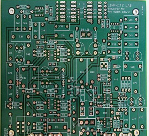
has caused a high concentration of interconnection lines because of the increase in integrated circuit packaging density. This makes the use of multiple substrates necessary. The layout of the printed circuit showed unforeseen design problems, such as noise, stray capacitance, and crosstalk. Therefore, the printed circuit board design must focus on minimizing the length of the signal line and preventing parallel routes. Obviously, in single-panel, or even double-panel, because the number of crossovers that can be achieved is limited, these requirements cannot be satisfactorily answered. Under the condition of a large number of interconnection and crossover requirements, the circuit board must be expanded to more than two layers in order to achieve a satisfactory performance, so a multi-layer circuit board is displayed. Therefore, the original intention of manufacturing multi-layer circuit boards is to select appropriate wiring paths for complex and/or noise-sensitive electronic circuits to provide more freedom.
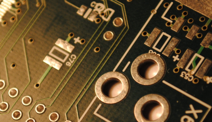
Two of the layers are on the outer surface, and the multilayer circuit board has at least three conductive layers. The remaining layer is integrated into the insulating board. The electrical connection is generally achieved through plated through holes on the cross-section of the circuit board. Unless otherwise stated, multi-layer printed circuit boards, like double-sided boards, are usually plated through-hole boards.
iPCB is a high-tech manufacturing enterprise focusing on the development and production of high-precision PCBs. iPCB is happy to be your business partner. Our business goal is to become the most professional prototyping PCB manufacturer in the world. Mainly focus on microwave high frequency PCB, high frequency mixed pressure, ultra-high multi-layer IC testing, from 1+ to 6+ HDI, Anylayer HDI, IC Substrate, IC test board, rigid flexible PCB, ordinary multi-layer FR4 PCB, etc. Products are widely used in industry 4.0, communications, industrial control, digital, power, computers, automobiles, medical, aerospace, instrumentation, Internet of Things and other fields.