PCB copy board technology implementation process in simple terms, is to first scan copy board circuit boards, record the details of the components, and components removed to make material list (BOM) and arrange the material purchasing, empty plate image is scanned into the software processing back into PCB copy board figure file, and then send a PCB file to plate plate making factory. After the board is made, the purchased components will be welded to the PCB board made, and then through the PCB test and debugging.
Specific steps of PCB copying board
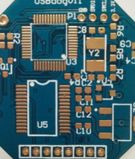
Step, get a PCB, first of all on the paper to record all the components of the model, parameters, and position, especially the
diode, three pipe direction, IC notch direction. Take two pictures of the position of the ski with your digital camera. Now the PCB circuit board more and more do above the diode triode some do not pay attention to simply see.

The second step, remove all the multilayer board copying parts, and remove the tin in the PAD hole. Clean the PCB with alcohol and place it into a scanner that scans at slightly higher pixels to get a sharper image. Then, polish the top and bottom layers lightly with water yarn paper until the copper film is shiny. Put them into the scanner, start PHOTOSHOP, and brush the two layers separately in color. Note that PCB must be placed horizontally and vertically in the scanner, otherwise the scanned image can not be used.
Third step, adjust the contrast and shade of the canvas to make the contrast between the part with copper film and the part without copper film strong, and then turn the picture to black and white, check whether the lines are clear, if not, repeat this step. If clear, the picture will be saved as black and white BMP format files top.bmp and bot.bmp, if found graphics problems can also be repaired and corrected with PHOTOSHOP.
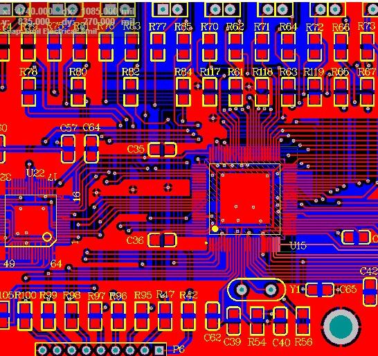
The fourth step is to convert the two BMP files into PROTEL files respectively, and transfer two layers into PROTEL. For example, the positions of PAD and VIA that have passed the two layers basically coincide, indicating that the previous steps have been done well. If there is any deviation, repeat the third step. Therefore, PCB board copying is a very need to bear the work, because a little problem will affect the quality and the matching degree of board copying.
Step 5, convert TOP layer BMP to TOP.PCB, make sure to convert SILK layer, that is the yellow layer, then you trace the line on TOP layer, and place the device according to the drawing of step 2. Delete the SILK layer after painting. Repeat until all layers are drawn.
Step 6, in PROTEL, call in top. PCB and bot. PCB, and combine them into one figure.
Step 7, use laser printer to print the TOP LAYER and the BOTTOM LAYER to transparent film (1:1 ratio), put the film on that PCB and compare if it is wrong, if it is right, you are done.
A copy of the original board was created, but it was only half done. Have a test even, the electronic technology performance that tests copy board is same as original board. If it's the same then it's really done.
Remark: If it is a multi-layer board but also carefully polished to the inside of the inner layer, at the same time repeat the third to the fifth step of copying board steps, of course, the graphics of the name is different, according to the number of layers to decide, the general double panel copying board is much simpler than the multi-layer board, multi-layer copying board is prone to misalignment, So the multilayer board copy board to be particularly careful and careful (the internal through hole and not through hole is prone to problems).
Double panel copying method
1. Scan the upper and lower layers of the circuit board to save two BMP pictures.
2. Open quickPC 2005, click "File" and "Open Base" to open a scanned image. Enlarge the screen with PAGEUP, see pad, place a pad according to PP, see the line according to PT line...... Just like a child drawing, draw it in the software and click "Save" to generate a B2P file.
3. Click "File" and "Open Base Map" to open the scan color map of another layer;
4. Click "File" and "Open" to open the previously saved B2P file. We can see that the newly copied board is superposed on this picture -- the same PCB board with holes in the same position, but the circuit connections are different. So we press "Options" - "Layer Settings" to turn off the display top line and silk screen here, leaving only multiple layers of holes.
5. The holes in the top layer are in the same position as the holes in the bottom layer. Now we can trace the lines in the bottom layer as we did in childhood. Click "Save" again - the B2P file now has the data at the top and bottom levels.
6. Click "File" "Export to PCB File", you can get a PCB file with two layers of data, which can be modified board or schematic diagram or directly sent to PCB plate factory for production.
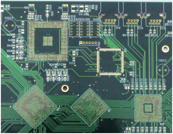
Multilayer board copy board method
In fact, the four board copy board is repeated copy two double panels, six is repeated copy three double panels...... The layers are daunting because we can't see the wiring inside. A sophisticated multilayer board, how do we see its inner universe? - layered.
Now there are many ways to layer, there are potion corrosion, tool stripping, but it is easy to layer too much, loss of data. Experience tells us that sandpaper is accurate.
When we finish copying the top and bottom layer of PCB, we usually use sandpaper to grind off the surface layer and show the inner layer. Sandpaper is the ordinary sandpaper sold in the hardware store, usually laid on the PCB, and then hold the sandpaper, evenly rubbed on the PCB (if the board is small, also can be laid on the sandpaper, with one finger to hold the PCB on the sandpaper friction). The point is to smooth it so that it's even.
Silk screen and green oil are generally wiped off, copper wire and copper skin should be wiped several times. Generally speaking, bluetooth board can be wiped in a few minutes, about ten minutes memory; Of course, with greater strength, it takes less time; Strength flower will have a little more time.
Grinding plate is the current layering with a common scheme, but also economic. We can find a discarded PCB to try. In fact, it is not technically difficult to grind the board, but it is a bit boring. It takes some effort, and there is no need to worry about grinding the board to your fingers.
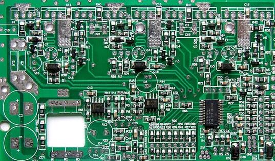
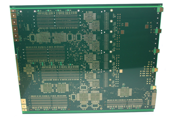
PCB diagram effect review
In the process of PCB layout, after the system layout is completed, the PCB diagram should be reviewed to see whether the system layout is reasonable and whether the effect can be achieved. It can usually be examined from the following aspects:
1. Whether the system layout can ensure the reasonable wiring or whether it can ensure the reliable wiring, whether it can ensure the reliability of the circuit work. During the layout, you need to have an overall understanding and planning of the signal direction and the power and ground network.
2. Whether the size of the printed board is consistent with the size of the processing drawings, whether it meets the requirements of PCB manufacturing process, and whether there are behavioral marks. This point needs special attention, many PCB circuit layout and wiring are designed very beautiful and reasonable, but neglect the positioning of the positioning plug-in, resulting in the design of the circuit can not be connected with other circuits.
3. Whether the components have conflicts in two-dimensional and three-dimensional space. Pay attention to the actual size of the device, especially the height of the device. In the weld-free layout of the component, the height generally cannot exceed 3mm.
4. Whether the layout of components is dense and orderly, neatly arranged, and whether all the cloth is finished. When laying out components, we should not only consider the direction and type of signals, and the areas that need attention or protection, but also consider the overall density of the device layout to achieve uniform density.
5. Whether the components that need to be replaced frequently can be easily replaced, and whether the plug-in board can be easily inserted into the equipment. It is necessary to ensure the convenience and reliability of replacing, connecting and inserting frequently changed components.