With the continuous increase in the output ratio of flexible PCBs and the application and promotion of rigid-flex PCBs, it is now more common to add soft, rigid or rigid-flex when talking about PCBs, and say that it is a PCB with several layers. Generally, a PCB made of a flexible insulating substrate is called a flexible PCB or a flexible PCB, and a rigid-flex composite PCB is called a rigid-flex PCB. It meets the needs of today's electronic products in the direction of high density and high reliability, miniaturization, and light weight. It also meets the strict economic requirements and the needs of market and technology competition.
First, the classification of flexible PCB and its advantages and disadvantages
1. Flexible PCB classification
Flexible PCBs are usually classified as follows according to the number and structure of conductors:
1.1 Single-sided flexible PCB
Single-sided flexible PCB has only one layer of conductor, and the surface can have a covering layer or no covering layer. The insulating base material used varies with the application of the product. Commonly used insulating materials include polyester, polyimide, polytetrafluoroethylene, and soft epoxy-glass cloth.
Single-sided flexible PCBs can be further divided into the following four categories:
1) Single side connection without covering layer
The conductor pattern of this kind of flexible PCB is on the insulating substrate, and the conductor surface has no covering layer. Like the usual single-sided rigid PCB. This type of product is the cheapest one, usually used in non-critical and environmentally friendly applications. The interconnection is realized by soldering, welding or pressure welding. It is commonly used in early telephones.
2) One-sided connection with cover layer
Compared with the previous type, this type only has an extra layer of coating on the surface of the wire according to customer requirements. The pads need to be exposed when covering, and it can simply be left uncovered in the end area. If precision is required, the form of clearance hole can be adopted. It is the most widely used and widely used single-sided flexible PCB, and is widely used in automotive instruments and electronic instruments.
3) Double-sided connection without covering layer
This type of connection board interface can be connected on the front and back of the wire. In order to achieve this, a via hole is opened on the insulating substrate at the pad. This via hole can be punched, etched or made by other mechanical methods at the required position of the insulating substrate. It is used for two-sided mounting of components, devices and occasions where soldering is required. There is no insulating substrate in the pad area of the via. Such pad area is usually removed by chemical methods.

4) With cover layer connected on both sides
The difference between this type and the previous type is that there is a covering layer on the surface. However, the cover layer has via holes, which allows termination on both sides and still maintain the cover layer. This kind of flexible PCB is made of two layers of insulating materials and a layer of metal conductors. It is used in the occasions where the covering layer and the surrounding devices need to be insulated from each other, and the ends need to be connected to both the front and back sides.
1.2 Double-sided flexible PCB
Double-sided flexible PCB with two layers of conductors. The application and advantages of this type of double-sided flexible PCB are the same as those of a single-sided flexible PCB, and its main advantage is to increase the wiring density per unit area. It can be divided into with or without metallized holes and with or without covering layer: a without metallized holes, without covering layer; b without metallized holes, with covering layer; c with metallized holes, without covering layer ; D There are metallized holes and covering layers. The double-sided flexible PCB without covering layer is rarely used.
1.3 Multilayer flexible PCB
Flexible multilayer PCB, like rigid multilayer PCB, adopts multilayer lamination technology to make multilayer flexible PCB. The simplest multilayer flexible PCB is a three-layer flexible PCB formed by covering two copper shielding layers on both sides of a single-sided PCB. This three-layer flexible PCB is equivalent to a coaxial wire or a shielded wire in electrical characteristics. The most commonly used multilayer flexible PCB structure is a four-layer structure, which uses metallized holes to realize interlayer interconnection. The middle two layers are generally the power layer and the ground layer.
Multilayer flexible PCB can be further divided into the following types:
1) A multilayer PCB is formed on a flexible insulating substrate, and the finished product is specified to be flexible: this structure usually bonds the two sides of many single-sided or double-sided microstrip flexible PCBs together, but the center The parts are not glued together, thus having a high degree of flexibility. In order to have the desired electrical characteristics, such as the characteristic impedance performance and the rigid PCB to which it is interconnected, each circuit layer of the multilayer flexible PCB component must be designed with signal lines on the ground plane. In order to have a high degree of flexibility, a thin, suitable coating, such as polyimide, can be used on the wire layer instead of a thicker laminated cover layer. The metallized holes enable the z-planes between the flexible circuit layers to achieve the required interconnection. This multilayer flexible PCB is most suitable for designs that require flexibility, high reliability, and high density.
2) A multilayer PCB is formed on a flexible insulating substrate, and the finished product can be flexed: this kind of multilayer flexible PCB is laminated with a flexible insulating material, such as polyimide film, to make a multilayer board. The inherent flexibility is lost after lamination. This type of flexible PCB is used when the design requires maximum use of the insulating properties of the film, such as low dielectric constant, uniform thickness of the medium, lighter weight, and continuous processing.
3) A multilayer PCB is formed on a flexible insulating substrate, and the finished product must be shapeable, not continuously flexible: this type of multilayer flexible PCB is made of soft insulating materials. Although it is made of soft materials, it is limited by electrical design. For example, for the required conductor resistance, a thicker conductor is required, or for the required impedance or capacitance, a thicker conductor is required between the signal layer and the ground layer. The insulation is isolated, so it is already formed in the finished application.
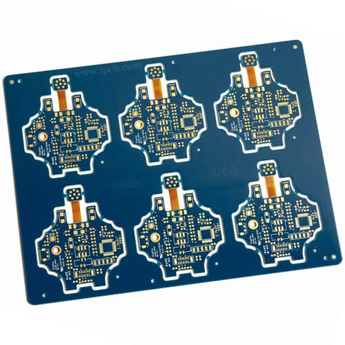
1.4 Rigid-flexible multilayer PCB
This type is usually on one or two rigid PCBs, and it contains the soft PCB that is necessary to form a whole. The flexible PCB layer is laminated in a rigid multi-layer PCB. This is to have special electrical requirements or to extend outside the rigid circuit to dynamize the Z-plane circuit mounting capability. This type of product has been widely used in electronic equipment that takes compression of weight and volume as the key, and must ensure high reliability, high density assembly and excellent electrical characteristics.
Rigid-flexible multi-layer PCBs can also bond and press the ends of many single-sided or double-sided flexible PCBs together to form a rigid part, while the middle is not bonded to form a soft part. The Z-side of the rigid part is interconnected with metallized holes. even. The flexible circuit can be laminated into the rigid multi-layer board. This kind of PCB is increasingly used in those occasions that require ultra-high packaging density, excellent electrical characteristics, high reliability and strictly limited volume.
2. Advantages
2.1 Flexibility
A significant advantage of the application of flexible PCB is that it can be more easily routed and installed in three-dimensional space, and it can also be crimped or folded for use. As long as it is curled within the allowable radius of curvature, it can withstand thousands to tens of thousands of times without being damaged.
2.2 Reduce the size
In the assembly and connection of components, the conductor cross-section of the flexible PCB is thin and flat compared with the use of conductive cables, which reduces the size of the conductor and can be formed along the casing, making the structure of the device more compact and reasonable, and reducing the size of the assembly. volume. Compared with rigid PCB, space can be saved by 60~90%.
2.3 Reduce weight
In the same volume, the flexible PCB can be reduced by about 70% compared with the wire and cable under the same current carrying capacity, and the weight can be reduced by about 90% compared with the rigid PCB.
2.4 Consistency of installation and connection
Use flexible PCB to install the connection, which eliminates the error when wiring with wires and cables. As long as the processing drawings are proofread and passed, all the winding circuits produced later will be the same. There will be no wrong connection when installing the cable.
2.5 Increased reliability
When flexible PCB is used for assembly and connection, because it can be routed on the three planes of X, Y, and Z, the transfer interconnection is reduced, the reliability of the entire system is increased, and the inspection of failures provides convenience.