Process test design market background in PCBA assembly
As a more mature processing and manufacturing method, the processing of circuit board manufacturers is entering the era of meager profit. The profit of PCBA processing is getting lower and lower, but the quality assurance requirements of PCBA processing are getting higher and higher. One of the companion requirements in PCBA assembly is consistency and correctness. To control the difference, mutation is not allowed. Poor quality in the assembly and manufacturing process has three aspects: design problems, material problems, and assembly problems. The first two items need to be taken in advance to prevent them from happening. Most of the problems in the assembly process, such as missing parts, damaged parts, wrong parts, offset, etc., can be visually inspected, but the welding quality is difficult to complete by visual methods. It is determined, and sometimes there may be failures such as the bomber, the board burst, and the malfunction of the PCBA delivered to the customer. According to the analysis and statistics of PCBA electrical equipment quality problems provided by China Saibao Laboratory Reliability Research and Analysis Center, the main assembly failure mode is poor welding, accounting for 57% of all poor assembly problems.

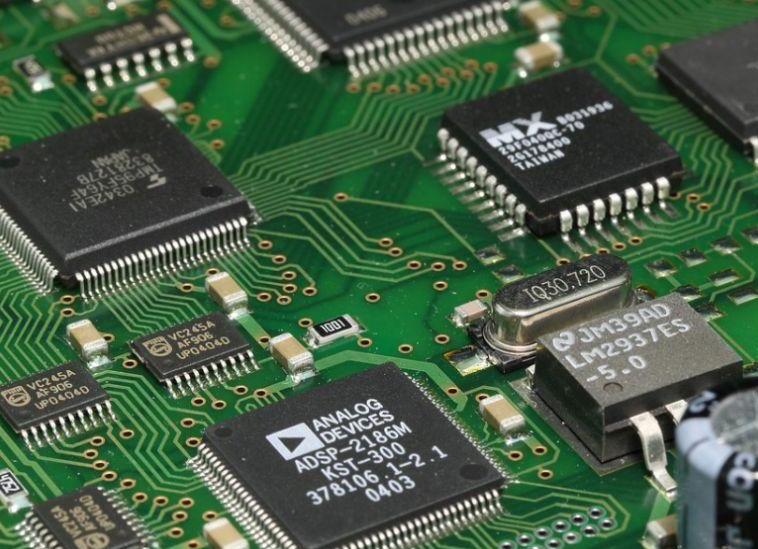
As the design of PCBA boards tends to be miniaturized, smaller devices, smaller problems, and more and more miniaturization (high density) of electronic assemblies, cause PCBA solder joint defects, difficult to detect and locate, and visualize Poor performance and maintainability, or even irreparable, the risk of potential failure also increases.
The traditional visual inspection and control of the PCBA assembly process cannot completely eliminate poor welding. Automatic X-ray non-destructive testing is also required. It has been promoted and applied in the Yangtze River Delta, the Pearl River Delta, and military production, and the effect is very good. However, the investment in adding equipment is relatively large. The previous year-on-year increase in labor costs has caused many small and medium-sized circuit board manufacturers to complain. Coupled with the continuous requirements of customers for processing quality, weak circuit board manufacturers have been unable to increase high costs. testing method.
iPCB is a high-tech manufacturing enterprise focusing on the development and production of high-precision PCBs. iPCB is happy to be your business partner. Our business goal is to become the most professional prototyping PCB manufacturer in the world. Mainly focus on microwave high frequency PCB, high frequency mixed pressure, ultra-high multi-layer IC testing, from 1+ to 6+ HDI, Anylayer HDI, IC Substrate, IC test board, rigid flexible PCB, ordinary multi-layer FR4 PCB, etc. Products are widely used in industry 4.0, communications, industrial control, digital, power, computers, automobiles, medical, aerospace, instrumentation, Internet of Things and other fields.