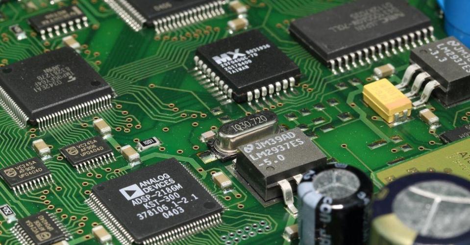
With the improvement of the performance of power semiconductor devices and the innovation of switching conversion technology, power electronic technology has been widely used in various power supply equipment. At present, the products of switching power supply tend to be small, high-speed PCB and high-density. This trend has caused electromagnetic compatibility problems to become more and more serious. The high-frequency switching process of voltage and current produces a large amount of EMI (electromagnetic interference). If this part of the interference is not restricted, it will seriously affect the normal operation of the surrounding electrical equipment. Therefore, the PCB design of the switching power supply is a vital aspect to solve the electromagnetic compatibility problem of the switching power supply. The reason why PCB is regarded as an indispensable and important component in the design of switching power supply is that it is responsible for the dual connection of the electrical and mechanical components of the switching power supply and is the key to reducing the EMI design of electronic equipment.

1 Electromagnetic interference in PCB design
1.1 Electromagnetic coupling interference
In circuit design, electromagnetic coupling interference mainly affects other circuits through conduction coupling and common mode impedance coupling. From the perspective of EMC design, switching power supply circuits are different from ordinary digital circuits, and have relatively obvious interference sources and sensitive lines. Generally speaking, the interference sources of switching power supplies are mainly concentrated on components and wires with large voltage and current rate of change, such as power FETs, fast recovery diodes, high-frequency transformers and wires connected to them. Sensitive lines mainly refer to control circuits and lines directly connected to interference measurement equipment, because these interference couplings may directly affect the normal operation of the circuit and the level of interference transmitted to the outside. The common-mode impedance coupling means that when the currents of two circuits pass through a common impedance, the voltage formed by the current of one circuit on the common impedance will affect the other circuit.
1.2 Crosstalk interference
The crosstalk interference between strips, wires, and cables in the printed circuit board (PCB) is one of the most difficult problems to overcome in the circuit of the printed circuit board. The crosstalk mentioned here is a crosstalk in a broader sense, no matter the source is useful signal or noise, crosstalk is expressed by the mutual capacitance and mutual inductance of wires. For example, a strip line on the PCB carries control and logic levels, and a second strip line close to it carries a low-level signal. When the parallel wiring length exceeds 10 cm, crosstalk interference is expected; When a long cable carries several sets of serial or parallel high-speed data and remote control lines, crosstalk interference also becomes a major problem. The crosstalk between adjacent wires and cables is caused by the electric field passing through mutual capacitance and the magnetic field passing through mutual inductance.
When considering the problem of crosstalk in the PCB strips, the main problem is to determine which of the electric field (mutual capacitance) and magnetic field (mutual inductance) coupling is more important. The determination of the coupling model mainly depends on the line impedance, frequency and other factors. Generally speaking, capacitive coupling is dominant at high frequencies, but if one or both of the source or receiver uses shielded cables and is grounded at both ends of the shield, magnetic field coupling will be dominant. In addition, low circuit impedance is generally lower at low frequencies, and inductive coupling is the main factor.
1.3 Electromagnetic radiation interference
Radiation interference is the interference introduced due to the radiation of electromagnetic waves in space. PCB electromagnetic radiation is divided into two types: differential mode radiation and common mode radiation. In most cases, the conducted interference produced by switching power supplies is dominated by common mode interference, and the radiation effect of common mode interference is much greater than differential mode interference. Therefore, reducing common mode interference is particularly important in the EMC design of switching power supplies. _)(^$RFSW#$%T
2 PCB interference suppression steps
2.1 PCB design information
When designing a PCB, you need to understand the design information of the circuit board, which includes the following:
(1) Number of devices, device size, and device packaging;
(2) Requirements for overall layout, device layout location, presence or absence of high-power devices, and special requirements for heat dissipation of chip devices;
(3) The speed of the digital chip, whether the PCB is divided into low-speed, medium-speed and high-speed areas, and which are the interface input and output areas;
(4) The type and speed of the signal line and the transmission direction, the impedance control requirement of the signal line, the direction of the bus speed and the driving situation, the key signal and the protection measures;
(5) Power supply type, ground type, noise tolerance requirements for power supply and ground, setting and division of power supply and ground plane;
(6) The type and speed of the clock line, the source and destination of the clock line, the clock delay requirement, and the longest wiring requirement.
2.2 PCB layering
First, determine the number of wiring layers and power supply layers required to implement the function within an acceptable cost range. The number of layers of the circuit board is determined by factors such as detailed functional requirements, immunity, separation of signal categories, device density, and bus wiring. At present, circuit boards have gradually developed from single-layer, double-layer, and four-layer boards to more-layer circuit boards. The design of multilayer printed PCB boards is the main measure to achieve electromagnetic compatibility standards. The requirements are:
(1) The distribution of separate power layer and ground layer can well suppress inherent common mode interference and reduce point source impedance;
(2) The power plane and the ground plane are as close as possible to each other, and the ground plane is generally above the power plane;
(3) It is best to lay out digital circuits and analog circuits in different layers;
(4) The wiring layer is preferably adjacent to the entire metal plane;
(5) Clock circuits and high-frequency circuits are the main sources of interference and should be dealt with separately.
2.3 PCB layout
The key to the EMC design of the printed circuit board is layout and wiring, which is directly related to the performance of the circuit board. The current EDA automation of circuit board layout is very low, requiring a lot of manual layout. Before layout, the PCB size that satisfies the function at the lowest possible cost must be determined. If the PCB size is too large and the device distribution is scattered during the layout, the transmission line may be very long, which will increase the impedance, reduce the anti-noise ability, and increase the cost. If the devices are placed in a centralized manner, the heat dissipation is not good, and the adjacent traces are prone to coupling crosstalk. Therefore, the layout must be carried out according to the circuit function unit, and factors such as electromagnetic compatibility, heat dissipation and interface must be taken into consideration at the same time. Some principles should be followed in the overall layout:
(1) Arrange each functional circuit unit according to the flow of the circuit signal to keep the signal flow in the same direction;
(2) Take the core component of each functional circuit unit as the center, and other components are laid out around it;
(3) Shorten the wiring between high-frequency components as much as possible and try to reduce their distribution parameters;
(4) The components that are susceptible to interference should not be too close to each other, and the input and output components should be far away;
(5) Prevent mutual coupling between power lines, high-frequency signal lines and general wiring.
2.4 PCB wiring
(1) Wiring principle
When wiring, classify all signal lines. Lay out the clock and sensitive signal lines first, and then route the high-speed signal lines. After ensuring that the vias for such signals are small enough and the distribution parameters are good, then route the general unimportant signal lines. The principles that should be followed are:
1) The wires of the input and output ends should be avoided as far as possible from the adjacent long distance parallel; in order to reduce the crosstalk of the long parallel wires, the line spacing can be increased, or the ground wire can be inserted between the wires;
2) The width of the circuit board should not be changed suddenly, and the wire should not be cornered suddenly. Keep the impedance of the circuit as continuous as possible. The corners of the printed transmission line generally follow a circular arc or form an angle of 135°;
3) Pay special attention to the distribution of power and ground wires of high-frequency circuits;
4) Reduce the wire loop area in the current flow process, because the external radiation of the current-carrying loop is proportional to the passing current, loop area and signal frequency;
5) Arrange more ground wire input pins scattered from each other on the circuit board plug, which helps to reduce the loop area and ground wire impedance of the circuit board pin wiring;
6) Reducing the length of the wire and increasing the width of the wire will help reduce the impedance of the wire.
(2) EMC wiring design of printed circuit
According to the interference electric field distribution diagram to carry on the printed circuit EMC wiring design, its basic idea is to put the sensitive circuit in the area with weaker interference. Then, according to the concept of "coupling coefficient" that has been proposed, the size of the distributed capacitance between the printed circuits is estimated in real time, and the PCB can be modified and improved in time during the design, which can effectively reduce the conduction interference of the PCB.
To choose a suitable layout plan, first calculate the interference intensity distribution map of the interference source. The switching frequency of most switching power supplies is between tens of kHz to several MHz, so the interference electric field on the PCB surface can be used for quasi-static field analysis. Under this assumption, the field quantity can be written as the product of independent space and time quantities. Therefore, the displacement current J (x, y, z, t) can be written as:
By solving Laplace equation (2), the spatial component of the potential at each point in space can be solved, and the corresponding spatial component of the displacement current density can be obtained by multiplying by the dielectric constant after the calculation. After visual calculation, the corresponding Research on electromagnetic compatibility of switching power supply PCB board
2.5 PCB anti-jamming circuit
For the digital control system of a large switching power supply, each logic device has a corresponding valve level and noise tolerance. As long as the external noise does not exceed the tolerance limit of the logic device, the system can work normally. However, once the noise or interference that invades the system exceeds a certain tolerance, the interference signal will be amplified and shaped by the logic device, which becomes an important cause of malfunction. The most sensitive of the single chip microcomputer system is the clock signal, reset signal and interrupt signal. These three signal lines should be paid special attention when laying out the PCB. While satisfying the function, the crystal oscillator with the lowest frequency should be selected.
The watchdog circuit is one of the anti-interference measures. When the strong electromagnetic interference, the grid spike interference causes the single-chip system to deadlock, the watchdog circuit can automatically detect and restore the program.
When the system is subject to strong interference and loses its normal working state, the data in the RAM will often be destroyed. Therefore, in addition to the careful design of the power supply system, a reliable RAM protection circuit must be designed.
The data bus, address bus and control bus of the circuit are exchanged for information. If the load capacity of the bus is increased, the signal waveform will be improved when the bus transmission is longer. At this time, a three-state buffer gate circuit needs to be configured as a bus driver. In addition, pay attention to ensuring the load balance of the bus.
The installation of pull-up resistors on the bus can improve the reliability of bus signal transmission, not only can increase the signal level, but also improve the bus's anti-electromagnetic interference ability, suppress electrostatic interference, and weaken reflected wave interference. When the chip has a built-in pull-up resistor, there is no need to install a pull-up resistor in an external circuit. For the chip pins on the circuit, fixing the unused input terminals at a high level can enhance the suppression of external electromagnetic interference.