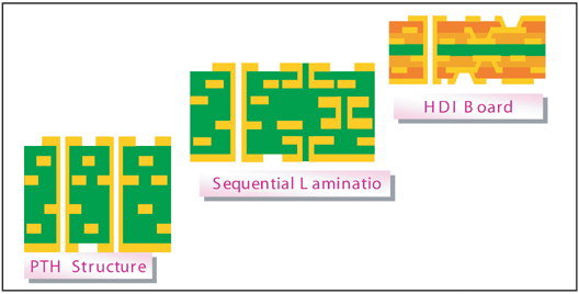
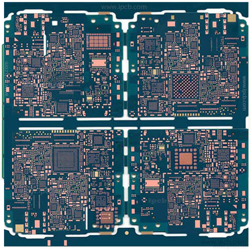
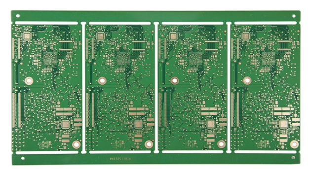
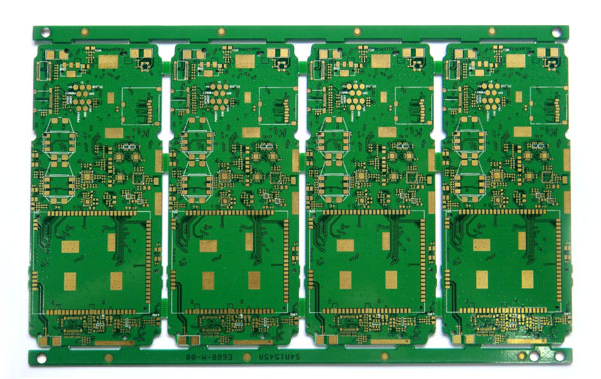
HDI defines HDI: short for high Density interconnection, high-density interconnection, non-mechanical drilling, micro-blind via hole ring is less than 6mil, inner and outer layer wiring line width/line gap is less than 4mil, and the pad diameter is not greater than 0.35mm The build-up multi-layer boardmanufacturing method is called HDI board.
Blind via: the abbreviation of Blind via, which realizes the connection between the inner layer and the outer layer. Buried via: the abbreviation of Buried via, which realizes the connection and conduction between the inner layer and the inner layer. The blind hole is mostly 0.05mm in diameter~ 0.15mm small holes, buried blind holes have laser hole formation, plasma etching and photo-induced hole formation, usually laser hole formation, and laser hole formation is divided into CO2 and YAG ultraviolet laser (UV).
2. HDI board material 1. HDI board material has RCC, LDPE, FR41) RCC: Resin coated copper abbreviation, resin coated copper foil. RCC is composed of copper foil and resin whose surface has been roughened, heat-resistant, anti-oxidation, etc., and its structure is shown in the following figure: (Used when thickness> 4mil) RCC resin layer, with FR-4 bonding sheet (Prepreg) Same processability. In addition, it is necessary to meet the relevant performance requirements of the build-up method multi-layer board, such as:
(1) High insulation reliability and microvia reliability;
(2) High glass transition temperature (Tg);
(3) Low dielectric constant and low water absorption;
(4) It has higher adhesion and strength to copper foil;
(5) The thickness of the insulating layer after curing is uniform and at the same time, because RCC is a new product without glass fiber, it is conducive to laser and plasma etching treatment, and it is conducive to the lightweight and thinning of the multilayer board.
In addition, the resin-coated copper foil has thin copper foils such as 12pm and 18pm, which is easy to process. 2) LDPE: 3) FR4 sheet material: used when the thickness is <=4mil. When using PP, generally use 1080, and try not to use 2116 PP2. Copper foil requirements: When the customer does not require it, the copper foil on the substrate is preferably 1 OZ in the traditional PCB inner layer, and the HDI board is preferably HOZ, and the inner and outer electroplated copper foils Use 1/3 OZ first.

3. Laser hole formation: CO2 and YAG UV laser hole formation The principle of laser hole formation: laser light is a powerful beam of light that is excited when the "ray" is stimulated by external sources, and the energy of infrared light or visible light has heat energy., UV light has another chemical energy. When it hits the surface of the work, there will be three phenomena of reflection (Refliction), absorption (Absorption) and penetration (Transmission), of which only the absorbed will have an effect. And its effect on the plate is divided into two different reactions: photothermal ablation and photochemical cracking. 1. YAG's UV laser hole formation: It can gather tiny beams, and the copper foil has a relatively high absorption rate. It can remove the copper foil and can be burned to micro blind holes below 4mil. When forming holes with CO2 lasers, resin will remain at the bottom of the hole. There is basically no resin remaining than the bottom of the hole, but it is easy to damage the copper foil at the bottom of the hole. The energy of a single pulse is small and the processing efficiency is low. (YAG, UV: Wavelength: 355, the wavelength is quite short, it can process very small holes, which can be absorbed by resin and copper at the same time) No special windowing process is required. 2. CO2 laser hole formation: using infrared CO2 laser machine, CO2 cannot be absorbed by copper, but can absorb resin and glass fiber, generally 4-6mil blind holes.
The hole forming method is as follows:
A. The Conformal Mask method of opening the copper window is to first press the RCC on the inner core board, then open the copper window, and then use laser light to burn off the substrate in the window to complete the micro-blind hole. The details are to first make the inner core board of FR-4, make it have blackened circuits and target pads on both sides, and then press it, and then remove the corresponding copper skin according to the copper etching film to remove the blind hole position and use CO2 The laser light burns the resin in the window, and the bottom pad can be hollowed out to form a micro blind hole. (The size of the copper window is the same as the blind hole.) This method was originally a patent of "Hitachi," and the general industry may have to be careful of legal issues when shipping to the Japanese market.
B. Large Conformal Mask The so-called "large window method" is to enlarge the copper window to be about 1 mil larger than the blind hole on one side. Generally, if the aperture is 6 mils, the large window can be opened to 8 mils. Our company uses this method for operation.
4. The laser drilling blind buried hole operation process is explained with 1+2+1 as an example
Production process: open material----open large copper window----drill L2~L3 buried hole-----remove slag ------electroplating buried hole------resin plug hole- ----Inner layer graphics-----Pressing ------L1-2&L4-3 layer Large Windows (copper window is 1mil larger than the blind hole diameter on one side) (etching)------- L1-2&L4-3 layer laser drilling blind hole-------Remove the slag twice-------Plating blind hole (pulse plating)------Resin plug hole----- - Grinding board + copper reduction------ mechanical drilling through hole --- normal process 2+4+2 process opening - L3~6 layer graphics - pressing - opening large copper window - L23&L76 layer Laser Buried hole-L26 mechanical drilling-Desmear-Plating buried hole-Resin plug hole-----L2, L7 layer pattern-Pressing-Open large copper window-L12&L87 layer Laser-Desmear----- Blind electroplating hole-----resin plug hole----grinding board + copper reduction----mechanical drilling----normal process