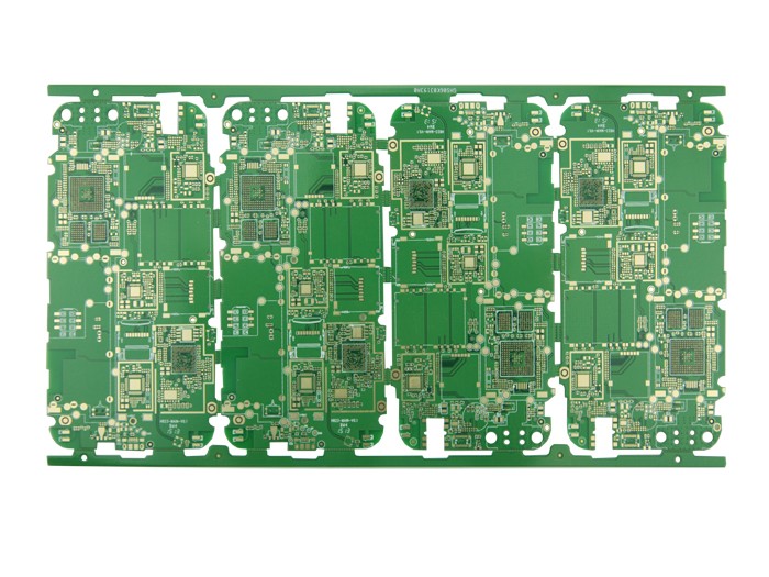
The via holes of the PCB board can be classified into the following types according to their functions:
1. Signal vias (via structure requirements have the least impact on the signal);
2. Power supply and ground vias (via structure requires the smallest distributed inductance of vias);
3. Thermal vias (via structure requires the minimum thermal resistance of vias);

The main functions of the hole are as follows:
1. Heat dissipation;
2. Connect the ground layer of the PCBmultilayer board;
3. The position of the via hole for layer change of high-speed signal;
For the ground hole spacing, generally only 1000mil is enough, the reasons are as follows:
Assume that the test range of EMI is up to 1Ghz. Then the wavelength of 1Ghz signal is 30cm, and 1/4 wavelength of 1Ghz signal is 7.5cm=2952mil. That is, if the spacing of the via holes can be less than 2952 mils, the ground connection can be well satisfied and a good shielding effect can be achieved.
Therefore, it is generally recommended to punch ground vias per 1000mil.
Principle Q&A Collection
1). What is the function and principle of adding a ground via hole near the via hole of the trace?
The via holes of the PCB board can be classified into the following types according to their functions:
1. Signal vias (via structure requirements have the least impact on the signal)
2. Power supply and ground vias (via structure requires the smallest distributed inductance of vias)
3. Thermal vias (via structure requires the minimum thermal resistance of vias)
The vias mentioned above belong to the grounding type vias. The effect of adding a grounding Via hole near the via hole of the trace is to provide the shortest return path for the signal. Note: The via hole where the signal changes layer is a discontinuity point of impedance, and the return path of the signal will be disconnected from here. In order to reduce the area surrounded by the return path of the signal, some ground must be laid around the signal via Vias provide the shortest signal return path and reduce signal EMI radiation. This radiation increases significantly with the increase of the signal frequency.
2). Under what circumstances should more ground holes be drilled? There is a saying: drilling more ground holes will destroy the continuity and integrity of the formation. The effect is counterproductive
First of all, if more holes are punched, the continuity and integrity of the power supply layer and the ground layer will be caused. This situation should be resolutely avoided. These vias will affect the power integrity, leading to signal integrity problems, which is very harmful. Holes in the ground usually occur in the following three situations:
1. Ground holes are used for heat dissipation;
2. The ground hole is used to connect the ground layer of the multilayer board;
3. The location of the via hole used for layer change of high-speed signals;
3). But all these situations should be carried out while ensuring the integrity of the power supply. That is to say, as long as the interval of ground holes is well controlled, is it allowed to drill more ground holes? Is it okay to drill ground holes at intervals of one-fifth of the wavelength?
If I make more ground holes in order to ensure the ground connection of the PCB multilayer board in PCB manufacturing, although there is no partition, will it affect the integrity of the ground layer and the power
If the power layer and the copper layer of the ground layer are not cut off, the effect is not big. In current electronic products, the general EMI test range is up to 1Ghz. Then the wavelength of the 1Ghz signal is 30cm, and the 1/4 wavelength of the 1Ghz signal is 7.5cm = 2952mil. That is to say, if the spacing of the vias can be less than 2952 mils, the ground connection can be well satisfied and a good shielding effect can be achieved.