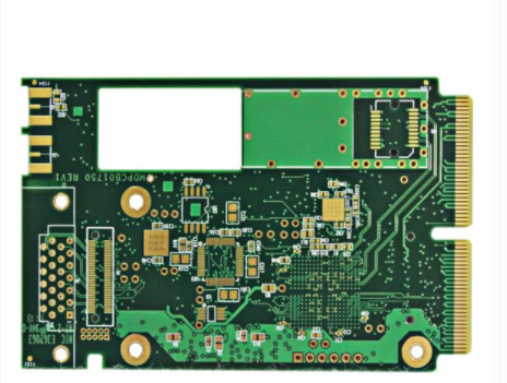
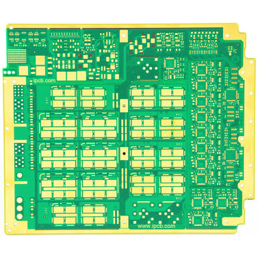
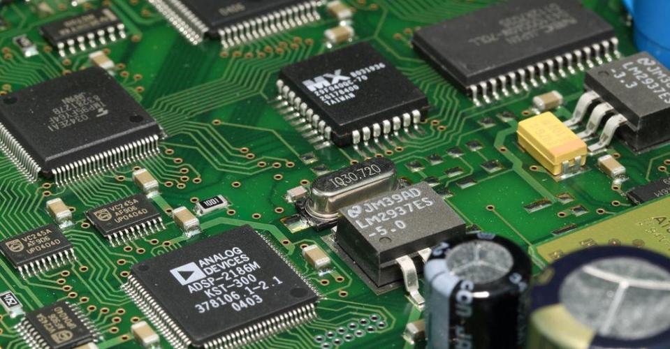
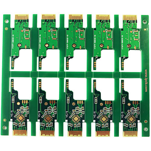
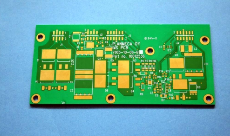
What is the implementation of via design in high-speed PCB proofing?

Most of the via design in high-speed PCB is through the analysis of the parasitic characteristics of the via. We can see that usually in the process of high-speed PCB design, often seemingly simple vias usually give the circuit design. Comes with great negative effects.
Therefore, in order to reduce the adverse effects caused by the parasitic effects of the vias, we can try our best to do the following in the design:
1. From the viewpoint of cost and signal quality, choose a reasonable size of the hole. For example, for the 6-10 layer memory module PCB design, it is better to use 10/20Mil (drilled/pad) vias, for some small high-density PCB circuit boards, You can also try to use 8/18Mil vias. Under current technical conditions, it is more difficult to use the smaller size of the hole. For power or ground vias, you can consider using a larger size to reduce impedance.
2. From the discussion of the above two formulas, it can be concluded that the use of a thinner PCB is beneficial to reduce the two parasitic parameters of the via.
3. The signal line has not changed on the PCB layer, that is to say, try not to use unnecessary vias.
4. The power and ground pins should be punched nearby, and the lead between the via and the pin should be as short as possible, because they will increase the inductance. At the same time, the power and ground leads should be as thick as possible to reduce impedance.
5. Place some grounded vias near the vias of the signal change layer, in order to provide the latest signal circuit. It is even possible to place a large number of redundant ground vias on the PCB board. Of course there is also a need for flexible design.
The via model discussed above is the case where everyone has a pad, and sometimes, we can reduce some of the keyboard or even cancel the layer. Especially in the case of a very high density of vias, it may cause a broken groove to form a circuit breaker in the copper layer.
To solve this problem, in addition to moving the position of the via hole, you can also consider the via hole in the pad to reduce the size of the copper layer.