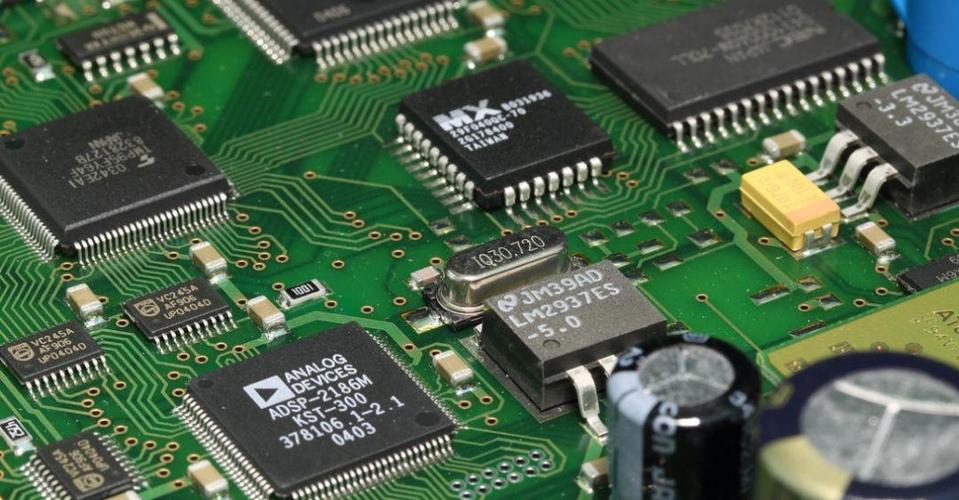
1. Find out the general working principle, working process and signal flow of its electrical circuit, and the position of each main component and core component on the PCB board.
2. It is recommended to look at the PCB board along the signal flow. It is okay to look forward (for example, starting from the tuner and looking backward) or backward (for example, when looking backward from the speaker). Sometimes the combination of the two is also suitable for the analysis of some circuits. The circuit must have branches. At this time, you need to look at the branches separately. If there are too many branches, you can mark them to distinguish the branches that have been seen. At the same time, you can pause at the marked place. Look at other branches or other parts of the circuit first., When the analysis reaches the original suspension point, it is considered that the analysis has completed the circuit at the time of suspension.
3. It’s best to look at the power supply and ground wire orientation first, and note down the positions of those power wires and ground wires as you look at them. When you analyze the components,
One end of the component is connected to the power or ground wire, even if you have finished reading it. The edge of the circuit board, the copper foil strip with the largest area, the place where the heat sink is connected to the copper skin, etc. (usually the negative electrode) is the ground wire. If these characteristics are not obvious, look at the filter capacitor of the power supply (for the positive power supply), that is, the negative connection of the electrolytic capacitor is the negative or ground of the circuit.
4. When looking along the signal flow, when you encounter a unit circuit or functional circuit, you should take the core components such as transistors and ICs as the center, and look at the components connected to each pole of the transistor and the connecting lines, and the peripheral components and circuits of each IC pin in turn. Of course, you can also divide the whole board into parts and divide it into several parts. Analyze the role of the component while looking at it, as well as the change of the signal (it is better to take into account what failures will occur if the component is damaged). When encountering an unfamiliar circuit, we must clarify its composition and circuit characteristics, and then contact similar typical circuits for comparison, viewing and analysis.
5. When looking at the PCB board, prepare a soldering iron and a multimeter, because when you encounter a transistor, you must know whether it is an NPN or PNP type.
and the order of the pins of each pole can analyze the circuit. With rich experience, I can judge the tube type and the position of each electrode when looking at most PCB boards. Sometimes it is necessary to identify the connection relationship of the circuit according to the internal structure of the component (such as switch, potentiometer, middle circle, etc.), which needs to be measured. For double-sided (multi-layer board) components, some of the traces and vias are often covered, which requires measurement, or even the removal of components, for intuitive observation.
6. Beginners must draw the schematic while looking at the PCB board. When drawing a schematic diagram, each component should be marked with its number,
In order to avoid omissions or misunderstandings, errors should be corrected in time. The component is on the front side (for a single panel, but there are also SMD components on the reverse side). The trace pad is on the reverse side. Keep in mind that when the front side is on the front side, the reverse side is in the opposite direction. For example, the capacitor on pin 1 of the IC (assuming it is on the left side of the IC) is on the right side of the IC part. There are also some experience to learn from: For example, a rectifier diode about 10mm long is horizontally on the front side, but it is still horizontally on the back side, but the direction of the positive and negative poles has changed. To find the pad and pin hole of this component on the reverse side, you can first look at the approximate position. At the reverse side, you can see that there are two holes in the horizontal position that are 10mm apart and slightly larger than the diode feet, which are the holes for this component. (When there is no other diode next to this diode), that is to say, when looking for the position of the pin hole of the negative component, it can be judged according to some characteristics of the component itself and its relative position with other components, if the components are all Arranged horizontally and vertically, on the reverse side you see a hole obliquely also has a hole, you think this is the two legs of a certain component, which is wrong.
7. There are also some PCB boards in consideration of the convenience of analysis. The front side is printed with blue and green strips in the same shape as the back side copper foil strips.
Or the symbol and number of the component are printed on the reverse side (single-sided copper foil welding surface). For such a board, the former can analyze most of the circuits by looking only at the front side, while for the latter, it is possible to analyze almost the complete board by looking only at the back side. This avoids the trouble of flipping the front and back and the mistakes caused by the board. In short, to see the specific process of the PCB board, you can first select some simple and familiar boards to view and draw, and then look at the complex PCB boards later. Only by repeated practice can a solid foundation be laid.