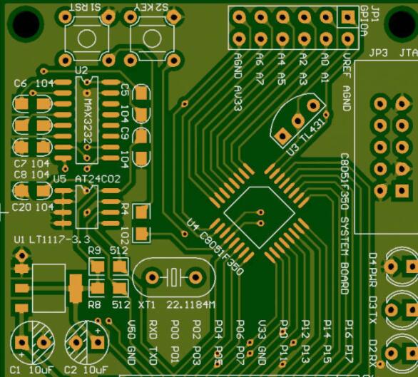
In the process of producing and processing PCB products, PCB factoriesneed to strictly inspect every link in order to produce reliable PCB products. Today, the editor of the PCB factory will tell you what inspections need to be done for PCB products with good quality, mainly including the following:
(1) Visual inspection.
Use visual inspection or magnifying glass to inspect the surface of the product (raw and auxiliary materials and PCB, etc.) for abnormal appearance, such as scars, colors, contaminants, residues, obvious open circuits and short circuits.
With the development of high density and refinement, it is necessary to use AOI (Automatic Optical Inspection Machine) to inspect the appearance of products, and even use scanning electron microscope (SEM) to inspect and measure copper foil surface micro-corrosion, inner surface oxidation treatment, and drilling Hole wall roughness, etc.
(2) Inspection of microsection cut surface.

Use a metallurgical microscope to observe whether there are any abnormalities or sizes in the plated through holes or via holes, such as the inside and outer layer patterns, etc., for evaluation, such as the roughness of the drilled hole wall, the de-drilling condition of the hole wall, the thickness distribution of the plating layer and the defect condition, and the layer Alignment and structure, and the situation after various aging tests, etc.
(3) Dimensional inspection.
Use tool microscope, coordinate measuring instrument or various measuring tools to measure the shape, hole diameter, hole position, wire width and spacing, land size, position relationship and flatness (warpage, deformation) of the board surface. Evaluation.
(4) Electrical performance test.
Various electrical performance test equipment are used to test the "on" and "off" (or "open", "short") of the loop (line), conductor resistance (conductor/via/inner connection) measurement, Insulation resistance (loop and loop, layer and layer, etc.) test, current resistance (wire, via or plated through hole) test, and voltage resistance (surface layer, layer and layer) test.
(5) Mechanical performance test.
Various test devices and jigs are used to measure the peel strength of copper foil, the peel strength of the copper plating layer (adhesion), the pull-off strength of plated through holes, ductility, bending resistance, bending resistance, solder resist and marking symbols. Adhesion and hardness test.
(6) Aging (lifetime reliability) test.
Various test devices are used to test and evaluate high and low temperature cycle resistance, thermal shock resistance (gas/liquid phase, such as float welding test), temperature and humidity cycle resistance, and interconnect stress test (IST).
(7) Other tests.
Various test devices are used to conduct tests and evaluations of combustion resistance, solvent resistance, cleanliness, solderability, soldering heat resistance (reflow soldering, reflow soldering, etc.), migration resistance, etc.
The editor of the PCB factory believes that as long as you strictly follow the detailed inspections above, you will be able to produce qualified and reliable PCB products.