What problems should be paid attention to in PCBA circuit board board drawing design
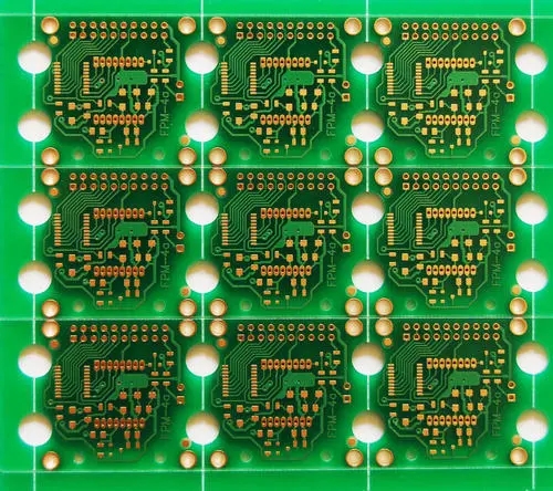
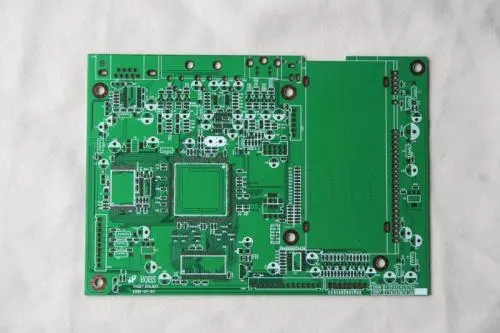
One of the most important design of PCBA circuit board in SMT processing is board drawing design, so what issues should be paid attention to for board drawing design? The following hundreds of achievements will be organized and introduced for everyone.
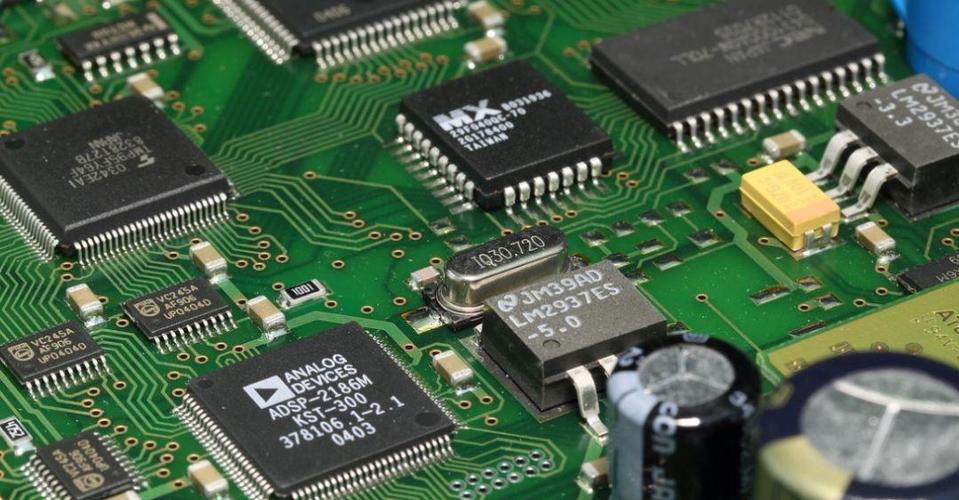
1. Create packages that are not in the package library. When designing the PCBA board drawing in the patch processing, if a component in the schematic diagram cannot find the package model in the package library, you need to use the component package model editor to create a new one, and ensure the package model of the component used It is complete in the package library (which can be multiple library files) to ensure the smooth progress of the PCBA design.
2. Set the design parameters of the PCB board drawing. According to the needs of the circuit system design, set the number of layers, size, color, etc. of the PCB board.
3. Load the network table. Load the netlist generated by the schematic, and automatically load the component package model into the PCB design window.
4. Layout. The method of combining automatic layout and manual layout can be used to place the component packaging model in an appropriate position within the PCB planning range, that is, to make the component layout neat, beautiful, and conducive to wiring.

5. Wiring. Set the wiring design rules and start automatic wiring. If the wiring is not completely successful, manual adjustments can be made.
6. Design rule check. Carry out design planning check on the designed PCB board (check whether the components overlap, whether the network is short-circuited, etc.), if there are errors, modify them according to the error report.
7. PCB board simulation analysis. Carry on simulation analysis to the signal processing of PCB board, mainly analyze the influence of layout and wiring on various parameters, so as to improve and modify.
8. Save the output. The designed PCB diagram can be saved, printed in layers, and output PCB design files. At present, the country has higher and higher requirements for environmental protection and greater efforts in link governance. This is a challenge but also an opportunity for PCB factories. If PCB factories are determined to solve the problem of environmental pollution, then FPC flexible circuit board products can be at the forefront of the market, and PCB factories can get opportunities for further development.
The Internet era has broken the traditional marketing model, and a large number of resources have been gathered together to the greatest extent through the Internet, which has also accelerated the development speed of FPC flexible circuit boards, and then as the development speed accelerates, environmental problems will continue to appear in PCB factories. In front of him. However, with the development of the Internet, environmental protection and environmental informatization have also been developed by leaps and bounds. Environmental information data centers and green electronic procurement are gradually being applied to the actual production and operation fields. From this point of view, the environmental protection problems of PCB factories can be solved from the following two points.