What are the standards in PCBA pad work
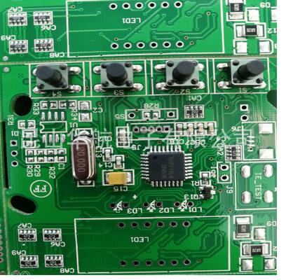
In SMT patch processing, the design of PCBA pads is very important. The design of the pads will directly affect the solderability, stability and heat transfer of the components, which is related to the quality of the patch processing. Therefore, when designing PCBA pads, It needs to be designed in strict accordance with the relevant requirements and standards. So what are the PCBA pad design standards? Below, Baiqiancheng Electronics will organize and introduce for everyone.
1. The shape and size design standard of PCBA pad:
1. Call the PCB standard package library.
2. The minimum single side of the pad is not less than 0.25mm, and the maximum diameter of the entire pad is not more than 3 times the component aperture.
3. Try to ensure that the distance between the edges of the two pads is greater than 0.4mm.
4. Pads with apertures exceeding 1.2mm or pad diameters exceeding 3.0mm should be designed as diamond-shaped or quincunx-shaped pads.
5. In the case of dense wiring, it is recommended to use oval and oblong connection plates. The diameter or minimum width of the single-sided board pad is 1.6mm; the weak-current circuit pad of the double-sided board only needs to add 0.5mm to the hole diameter. Too large a pad may easily cause unnecessary continuous soldering.

2. PCBA pad via hole size standard:
The inner hole of the pad is generally not less than 0.6mm, because the hole smaller than 0.6mm is not easy to process when punching the die. Usually, the diameter of the metal pin plus 0.2mm is used as the inner hole diameter of the pad, such as the diameter of the metal pin of the resistor When it is 0.5mm, the diameter of the inner hole of the pad corresponds to 0.7mm, and the diameter of the pad depends on the diameter of the inner hole.
Three, the reliability design points of PCBA pads:
1. Symmetry. To ensure the balance of the surface tension of the molten solder, the pads at both ends must be symmetrical.
2. Pad spacing. Too large or too small pad spacing will cause soldering defects. Therefore, ensure that the spacing between component ends or pins and pads is appropriate.
3. The remaining size of the pad. The remaining size of the component end or pin and the pad after the overlap must ensure that the solder joint can form a meniscus.
4. The width of the pad should be basically the same as the width of the component tip or pin.
Correct PCBA pad design, if there is a small amount of skew during patch processing, it can be corrected due to the surface tension of the molten solder during reflow soldering. And if the PCB pad design is incorrect, even if the placement position is very accurate, soldering defects such as component position offset and suspension bridges will easily occur after reflow soldering. Therefore, great attention should be paid to the PCB pad design.