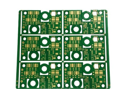
In order to prevent PCB from deformation as much as possible during PCB welding, most PCB manufacturers require PCB designers to fill copper sheet or grid ground wire in the open area of PCB.
However, our engineers dare not use this "filling" easily, perhaps because they have suffered "hardships" in PCB debugging, or the experts have not given a clear conclusion.
Whether copper plating is "more advantages than disadvantages" or "more disadvantages than advantages", this paper explains this problem from the perspective of actual measurement.
The following measurement results are obtained by emscan electromagnetic interference scanning system (www.emcdir. Com). Emscan enables us to see the distribution of electromagnetic field in real time. It has 1218 near-field probes and uses electronic switching technology to scan the electromagnetic field generated by PCB at high speed. It is the only electromagnetic field near-field scanning system using array antenna and electronic scanning technology in the world, and it is also the only system that can obtain complete electromagnetic field information of the measured object.
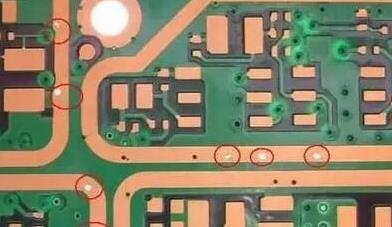
Let's look at a measured case. On a multi-layer PCB, the engineer coated a circle of copper around the PCB, as shown in Figure 1. In this copper coating treatment, the engineer only placed a few vias at the beginning of the copper sheet to connect the copper sheet to the formation, and no vias were drilled elsewhere.

Electromagnetic field caused by copper coating with poor grounding of PCB
Fig. 1 electromagnetic field generated by copper coating with poorly grounded PCB
In the case of high frequency, the distributed capacitance of the wiring on the printed circuit board will play a role. When the length is greater than 1 / 20 of the corresponding wavelength of the noise frequency, the antenna effect will be generated, and the noise will be emitted outward through the wiring.
From the above actual measurement results, there is an interference source of 22.894mhz on the PCB, and the laid copper sheet is very sensitive to this signal. It receives this signal as a "receiving antenna". At the same time, the copper sheet transmits a strong electromagnetic interference signal to the outside as a "transmitting antenna".
We know that the relationship between frequency and wavelength is f = C/ λ.
Where f is the frequency, in Hz, λ Is the wavelength, in M, and C is the speed of light, equal to 3 * 108 M / S
For 22.894mhz signal, its wavelength λ Is: 3 * 108 / 22.894m = 13m. λ/ 20 is 65cm.
The copper coating on this PCB is too long, exceeding 65cm, resulting in antenna effect.
At present, chips with rising edge less than 1ns are widely used in our PCB. Assuming that the rising edge of the chip is 1ns, the frequency of electromagnetic interference generated by the chip will be as high as fknee = 0.5 / TR = 500MHz. For a 500MHz signal, the wavelength is 60cm, λ/ 20=3cm. In other words, 3cm long wiring on PCB may form "antenna".
Therefore, in high-frequency circuits, do not think that the ground wire is grounded somewhere, which is "ground wire". Must be less than λ/ 20, through holes in the wiring, and "well grounded" with the ground plane of the multilayer board.
For general digital circuits, the "ground filling" of component surface or welding surface shall be drilled at a spacing of 1cm to 2cm to realize good grounding with the ground plane, so as to ensure that the "ground filling" will not have the influence of "disadvantages".
Therefore, we extend as follows:
Ø do not apply copper in the open area of wiring in the middle layer of multi-layer board. Because it's hard for you to make this copper coating "well grounded"
Ø for a PCB, no matter how many kinds of power supplies there are, it is recommended to use power division technology and only use one power layer. Because the power supply and ground are the same as "reference plane", the "good grounding" of power supply and ground is realized through a large number of filter capacitors. Where there is no filter capacitor, there is no "grounding".
Ø the metal inside the equipment, such as metal radiator and metal reinforcing strip, must be well grounded.
Ø the heat dissipation metal block of the three terminal voltage regulator must be well grounded.
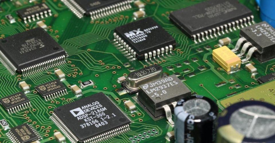
The grounding isolation belt near the crystal oscillator must be well grounded.
Conclusion: if the grounding problem of copper coating on PCB is handled well, it must be "advantages outweigh disadvantages". It can reduce the return area of signal line and reduce the external electromagnetic interference of signal.