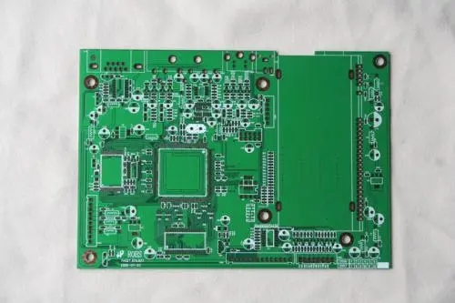
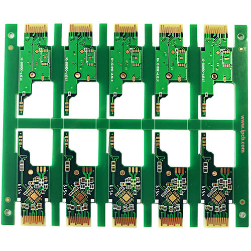
PCB device layout is a very tricky thing, but if you master its principles, then everything will become very simple. Here are some PCB board device layout principles summarized daily.

1. The I/O drive device is as close as possible to the edge of the printed board and to the lead-out connector;
2. According to the reasonable division of electrical performance, it is generally divided into: digital circuit area (that is, afraid of interference and interference), analog circuit area (fear of interference), power drive area (interference source);
3. Circuits that complete the same function should be placed as close as possible, and each component should be adjusted to ensure the most concise connection; at the same time, adjust the relative position between the functional blocks to make the connection between the functional blocks the most concise;
4. For high-quality components, the installation location and installation strength should be considered; heating components should be placed separately from temperature-sensitive components, and thermal convection measures should be considered when necessary;
5. Between the power input pin of each integrated circuit and the ground, a decoupling capacitor (generally a monolithic capacitor with good high-frequency performance is used); when the board space is dense, one can also be added around several integrated circuits Tantalum capacitor;
6. The layout requirements should be balanced, dense and orderly, not top-heavy or heavy;
7. The clock generator (such as crystal oscillator or clock oscillator) should be as close as possible to the device that uses the clock;
8. A discharge diode should be added to the relay coil.
The advantages of using multi-layer PCBs in high-speed circuit board design
Multi-layer circuit boards are recommended in the design of high-speed circuit boards. First of all, the multi-layer PCB allocates inner layers to power and ground, so it has the following advantages:
The power supply is very stable;
The circuit impedance is greatly reduced;
·The wiring length is greatly shortened.

In addition, from a cost point of view, when the same area is used for cost comparison, although the cost of a multi-layer PCB is higher than that of a single-layer PCB, if other factors such as the miniaturization of the circuit board and the convenience of reducing noise are taken into account, the multi-layer circuit board The cost difference between the two and the single-layer circuit board is not as high as expected. When simply calculating the area cost of the circuit board according to the data we know, the area of the double-layer circuit board that can be purchased by the daily yuan is about 462mm2, and the area of the 4-layer circuit board is 26mm2, which means that the same circuit is designed, if 4 layers The use area of the circuit board can be reduced to 1/2 of the double-layer board, so the cost is the same as that of the double-layer circuit board. Although multiple layers in batches will affect the cost per unit area of the circuit board, there is still not a 4 times price difference. If a price difference of more than 4 times occurs, as long as you can try to reduce the use area of the circuit board, and try to reduce it to 1% of the double-layer board. /4 or less is fine.