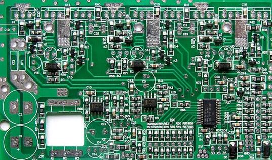
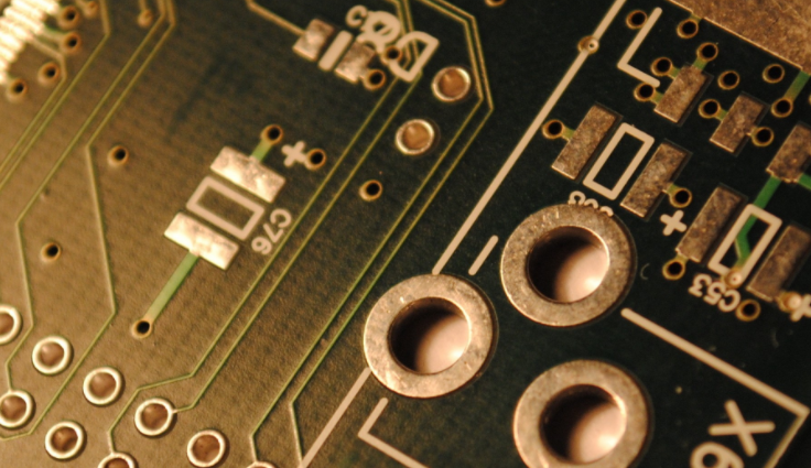
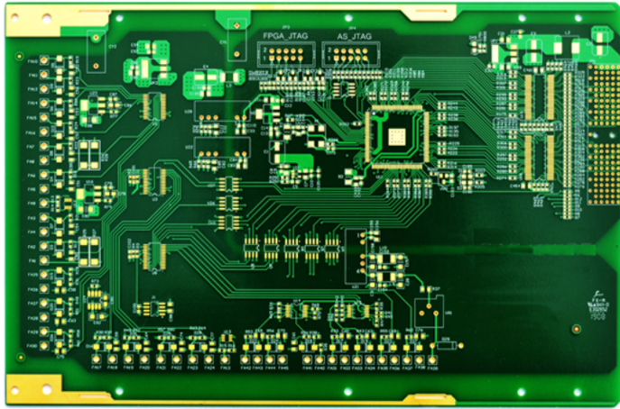
PCB multilayer circuit board layered blistering
In the multi-variety, small-batch military production process of circuit boards, many products also require lead-tin plates. Especially for the high-precision printed PCB multi-layer boards with many varieties and very few quantities, if the hot-air leveling process is adopted, it will obviously increase the manufacturing cost, the processing cycle is also long, and the construction is also very troublesome. For this reason, lead-tin plates are usually used in PCB manufacturing, but the quality problems caused by circuit board processing are more. The major quality problem is the quality problem of delamination and blistering after infrared thermal melting of the lead-tin coating on the multilayer printed circuit board.
In the pattern electroplating process method, the printed PCB multilayer board generally adopts the tin-lead alloy layer, which is not only used as the pattern metal anti-corrosion layer, but also provides a protective layer and a soldering layer for the lead-tin board. Because of the pattern plating-etching process, after the circuit pattern is etched, both sides of the wire are still copper layers, which are prone to contact with air to produce an oxide layer or be corroded by acid and alkali media.

In addition, since the circuit pattern is prone to undercut during the etching process, the tin-lead alloy plating part is suspended and a suspension layer is produced. But it is easy to fall off, causing short circuit between wires. The use of infrared hot melt technology can make the exposed copper surface get extremely good protection. At the same time, the tin-lead alloy coating on the surface and in the hole can be recrystallized after infrared heat melting, making the metal surface shiny. It not only improves the solderability of the connection point, but also ensures the reliability of the connection between the components and the inner and outer layers of the circuit. However, when used for infrared heat melting of multilayer printed circuit boards, due to the high temperature, the delamination and blistering between layers of the PCB multilayer circuit board is very serious, which results in the yield of the multilayer printed circuit board. Extremely low. What causes the layered blistering quality problem of multilayer printed circuit boards?
PCB multilayer circuit board causes:
(1) Insufficient glue flow;
(2) The inner circuit board or prepreg is contaminated;
(3) Improper suppression results in the accumulation of air, moisture and pollutants;
(4) Poor blackening treatment of inner circuit or surface contamination during blackening;
(5) Excessive flow of glue-almost all of the glue contained in the prepreg is extruded out of the board;
(6) Due to insufficient heat during the pressing process, the cycle is too short, the quality of the prepreg is poor, and the function of the press is not correct, resulting in problems with the degree of curing;
(7) In the case of non-functional requirements, the inner layer board minimizes the appearance of large copper surfaces (because the bonding force of the resin to the copper surface is much lower than the bonding force of the resin to the resin);
(8) When vacuum pressing is used, the pressure is insufficient, which will damage the glue flow and adhesion (the multi-layer board pressed by the low pressure also has less residual stress).
PCB multilayer circuit board solution:
(1) The inner circuit board needs to be baked to keep dry before being laminated.
Strictly control the process procedures before and after pressing to ensure that the process environment and process parameters meet the technical requirements.
(2) Check the Tg of the pressed multilayer board, or check the temperature record during the pressing process.
The pressed semi-finished product is then baked at 140°C for 2-6 hours, and the curing process is continued.
(3) Strictly control the process parameters of the oxidation tank and cleaning tank of the blackening production line and strengthen the inspection of the surface quality of the board.
Try the double-sided copper foil (DTFoil).
(4) The cleaning management of the work area and storage area shall be strengthened.
Reduce the frequency of hand-carrying and continuous board removal.
Various bulk materials need to be covered to prevent contamination during the lamination operation.
When the tool pin must be lubricated and released with a surface treatment, it should be separated from the lamination operation area and cannot be carried out in the lamination operation area.
(5) Appropriately increase the pressure intensity of suppression.
Appropriately slow down the heating rate and increase the glue flow time, or add more kraft paper to ease the heating curve.
Replace the prepreg with a higher flow rate or longer gel time.
Check whether the surface of the steel plate is flat and free of defects.
Check whether the length of the positioning pin is too long, causing the heating plate not to be tightly attached and insufficient heat transfer.
Check whether the vacuum system of the vacuum multilayer press is in good condition.
(6) Appropriately adjust or reduce the pressure used.
The inner layer board before pressing needs to be baked and dehumidified, because the moisture will increase and accelerate the flow of glue.
Switch to prepregs with lower flow rate or shorter gel time.
(7) Try to etch away the useless copper surface.
(8) Gradually increase the pressure intensity used for vacuum pressing until it passes five float welding tests (each time is 288°C, 10 seconds). (Explained by PCB manufacturer)