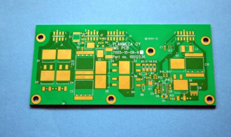
HDI board and blind buried via circuit board
HDI is a product of circuit boards, the full name is highDensityInterconnection, high-density interconnection boards. At present, high-end electronic products are generally HDI board products.
Blindvias: Blind vias are vias that connect the inner traces of the PCB to the traces on the surface of the PCB. This hole does not penetrate the entire board.
Buried vias: Buried vias are the type of vias that only connect the traces between the inner layers, so they are invisible from the surface of the PCB.
With the current development of portable product design in the direction of miniaturization and high density, PCB design is becoming more and more difficult, and higher requirements are placed on the PCB production process. In most of the current portable products, the BGA package with a pitch of less than 0.65mm uses the design process of blind and buried vias. So what is the blind and buried via?

Blindvias: Blind vias are vias that connect the inner traces of the PCB with the traces on the surface of the circuit board. This hole does not penetrate the entire board.
Buried vias: Buried vias are the type of vias that only connect the traces between the inner layers, so they are invisible from the surface of the PCB.
The circuit board with buried blind vias is not necessarily an HDI circuit board, but generally HDI boards have blind vias, but buried vias are not necessarily the case. It depends on the order and pressure of your circuit board product.
described as follows:
The first order and the second order of the 6-layer circuit board are for the board that needs laser drilling, that is, the HDI board.
6-layer circuit board first-order HDI board refers to blind holes: 1-2, 2-5, 5-6. That is, 1-2, 5-6 need laser drilling.
6-layer circuit board second-order HDI board refers to blind holes: 1-2, 2-3, 3-4, 4-5, 5-6. That is, 2 laser drilling is required.
First drill 3-4 buried holes, then press 2-5, then drill 2-3, 4-5 laser holes for the first time, then press 1-6 for the second time, then drill 1-2 for the second time, 5-6 laser holes. Finally, the through holes are drilled. It can be seen that the second-order HDI board has been pressed twice and laser drilled twice.
In addition, second-order HDI boards are also divided into: second-order HDI boards with wrong holes and second-order HDI boards with stacked holes. Board refers to the blind holes 1-2 and 2-3 stacked together, for example: blind: 1-3, 3-4, 4-6.
and so on, third-order, fourth-order... are all the same.
iPCB is a high-tech manufacturing enterprise focusing on the development and production of high-precision PCBs. iPCB is happy to be your business partner. Our business goal is to become the most professional prototyping PCB manufacturer in the world. Mainly focus on microwave high frequency PCB, high frequency mixed pressure, ultra-high multi-layer IC testing, from 1+ to 6+ HDI, Anylayer HDI, IC Substrate, IC test board, rigid flexible PCB, ordinary multi-layer FR4 PCB, etc. Products are widely used in industry 4.0, communications, industrial control, digital, power, computers, automobiles, medical, aerospace, instrumentation, Internet of Things and other fields.