The motivation of PCB board to "face up to difficulties" is introduced as follows:
The environment facing economic development in 2019 is more complex and severe, mainly due to the uncertainty of the international economic situation. The uncertainty of the world economy is reflected in the uncertainty of economic policies in the US economic strength, such as requiring the manufacturing industry to return to the United States, the monetary policy of the Federal Reserve, the compression of immigration policies, and the uncertainty of the European economy, such as the difficulties of economic recession over the years Rising, uncertain whereabouts, undecided Brexit plan, uncertainties in reform of multilateral trade rules; tensions in Sino-US economic and trade relations, and uncertain frictions.

In the face of uncertainty, PCB companies should enhance the vitality of micro-subjects, give full play to the subjective initiative of enterprises and entrepreneurs, and propose the courage, strength and perseverance to overcome external uncertainties. Uncertainty exists in the external environment, and our personal business cannot be reversed.
However, we can still see some enthusiasm beyond uncertainty. The general trend of social progress and economic development is obvious. People’s rich and colorful material needs are universal. The development of the Internet and the intelligent electronic information industry is active. The electronic circuits in the electronic information industry are indispensable, and electronic circuits are adapted to The new requirements of electronic equipment are objective. On this basis, there is a certain enthusiasm for the development of printed circuit technology!
5G equipment requires a new generation of printed circuit boards
An important feature of PCBs used in 5G devices is high-frequency and high-speed signal transmission. Therefore, PCBs can meet the requirements of high-frequency and high-speed from design, material to manufacturing. From the perspective of signal integrity, in addition to optimizing the power distribution network, keeping the signal line impedance constant and anti-electromagnetic interference, PCB design must also make a good choice of substrate materials, while considering the dielectric loss angle tangent and dielectric constant, and copper surface Roughness.
The final coating and resistance welding layer on the surface of the high-frequency PCB will also affect the performance of the PCB circuit. The designer should also correctly select the final coating and resistance welding layer of the PCB.
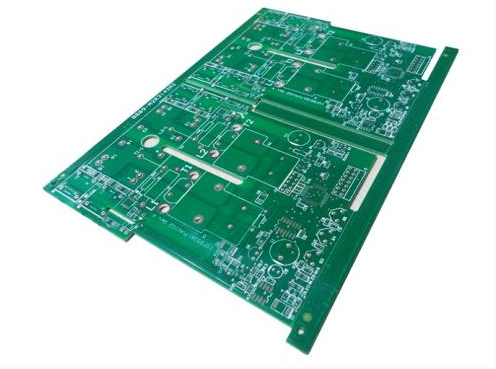
From the perspective of PCB materials, 4G has not changed much from 2G to 3G in the past, because there is only a small difference in frequency. The PCB substrate basically chooses FR-4 as the dielectric material, and does not particularly emphasize the performance of the material.
At the beginning of 5G, the frequency was 6GHz, and then to 28GHz millimeter wave. The material requirements have changed greatly. Because the frequency is much higher, the material loss is much smaller, and the copper foil must be thinner and smoother.
High-frequency laminates show differences from FR-4 in terms of dielectric constant (DK), dielectric loss (DF), Dk thermal coefficient (TCDk), moisture absorption, heat resistance and thermal conductivity, copper surface roughness, etc. .
The main factor affecting Dk and Df in PCB substrates is the type of resin, and low-loss materials such as PTFE and liquid crystal polymer (LCP) have advantages.
It is now confirmed that the LCP substrate PCB has a broad market in the RF and MW fields, including flexible boards, rigid bonding boards, packaging boards and high-level multilayer boards, so the application of LCP substrates is increasing.
In addition to the resin composition to determine the dielectric properties, the reinforced material glass fiber cloth is also an important factor. The type of glass fiber cloth is different between E glass cloth and NE glass cloth. The application of NE glass fiber weaves densely, which can reduce attenuation and enhance signal integrity. sex.
HDI boards represented by smartphones are often denser and more advanced in the manufacturing process, which is reflected in class-loading boards (SLP) and improved semi-additive (mSAP). The main feature of SLP is the line width/line spacing (L/S) density between the HDI board and the carrier board, which is currently between 30/30μm and 15/15μm; the manufacturing process uses coated copper foil (<5μm) As the seed layer, then the pattern plating and flashover of MSAP, MSAP becomes a new generation HDI board (level load board)
At present, many companies in the PCB industry are building or expanding factories, and they must have smart factory design concepts to keep up with the pace of the times. It is worth noting that the current development speed of electronic technology is faster than ever before, and our electronic circuit industry has a broad market prospect.