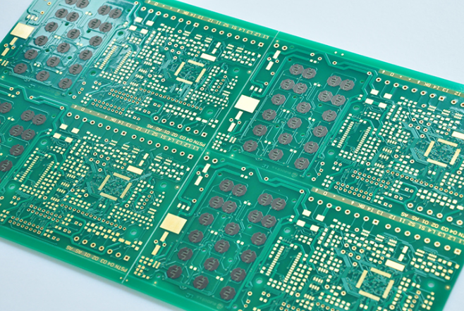
Introduction to buried blind holes of PCB circuit boards
One, the definition of the buried blind hole of the PCB circuit board
2. Related IPC standards for buried blind vias of PCB circuit boards
Blind hole resin filling (IPC-600G)
PCB circuit board buried blind hole copper thickness requirements (IPC-6012B)
3. Difficulties in the processing of buried and blind vias
thin plate plating
Multiple plating, copper thickness uniformity and etching difficulty increase
Alignment of blind holes and through holes of PCB circuit board
Warpage
The shrinkage of the inner core board when pressed twice or more
Blind hole filling
Blind hole removal glue
Fourth, the key points of PCB circuit board buried blind hole processing control
inner drilling

When stacking the board, the board must be flat and no bowing
The presser foot needs to press the aluminum sheet tightly during processing to prevent large burrs
Thin plate (<3mm) is used to pad underneath when polishing, to prevent polishing deformation
The inner layer is copper-immersed, thickened
The cleaning of copper sinking front grinding machine
When the whole plate is plated, <5mm core plate is processed by thin plate frame
After plating, all the plates are polished with 1500# sandpaper
The copper thickness of the hole is processed according to the IPC standard, and the engineering MI will require the copper thickness to be clearly stated
Inner graphics, inspection
Wear scar test is required when pre-processing the grinding plate. The <15mm plate is micro-etched on the IS machine, and then the first set of grinding brushes are lightly ground on the cosmic plate grinding machine to ensure that the surface of the plate is not oxidized.
The alignment is centered and symmetrical to ensure that there is no damage to the PAD at the four corners of the board.
The four corners of the inspection board should not be broken.
Lamination
Thin plate pay attention to adjust the height of the empty riveting.
The steel plate is cleaned to prevent the glue in the dents from being dirty.
The release film should not have wrinkles, too much glue, which will affect the glue removal effect
When drilling the target, the blind hole layer faces upward to drill the target.
When drilling the target, turn it over every 5PNL to check whether there is any deviation.
Blind hole filling cannot use S1000B and S1000-2B PP.
glue removal
Blind hole removal is done in the sinking copper for drilling dirt, and after the drilling dirt is removed, the plate is polished on the space grinding machine.
The unremoved board can only be polished by hand
micro-eclipse
Measure the copper thickness of the board surface before micro-etching, if there is a difference (between the average value of the board surface ≥10um), classify the micro-etching.
Confirm the parameters of the first piece before micro-etching, to ensure that the number of micro-etching is even number, and the number of passes on the front and back of the micro-etching is the same.
During micro-etching, the copper thickness of the board surface shall be measured randomly. If there is any abnormality, the processing shall be stopped in time and the processing parameters shall be readjusted.
Add chemicals according to the PNL number during micro-etching to keep the micro-etching liquid stable.
drilling
When installing the board, hold the board with both hands, and insert the positioning nails horizontally. Don't push it into it by force to prevent damage to the target hole.
Check the test hole for the first part before processing, confirm the deviation and shrinkage, if there is any damage, notify the engineer to deal with it.
Outer graphics, inspection
Use the yellow film to check the alignment of the through hole and the blind hole with a tenfold lens. Refer to the blind hole alignment PAD at the four corners of the board.
When inspecting the outer layer, use a ten-fold lens to check the alignment of the blind hole, and the ring shall not be broken.
Etch
Find out and measure the minimum line width before etching, and make the first product after confirming that it is qualified.
When processing, pay attention to check the etching effect at the edge of the blind hole and the BGA to prevent under-corrosion and unclean etching.
iPCB is a high-tech manufacturing enterprise focusing on the development and production of high-precision PCBs. iPCB is happy to be your business partner. Our business goal is to become the most professional prototyping PCB manufacturer in the world. Mainly focus on microwave high frequency PCB, high frequency mixed pressure, ultra-high multi-layer IC testing, from 1+ to 6+ HDI, Anylayer HDI, IC Substrate, IC test board, rigid flexible PCB, ordinary multi-layer FR4 PCB, etc. Products are widely used in industry 4.0, communications, industrial control, digital, power, computers, automobiles, medical, aerospace, instrumentation, Internet of Things and other fields.