Some requirements for PCB circuit board pad design
Pad type
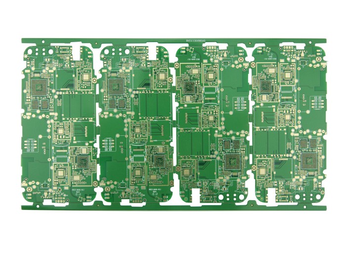
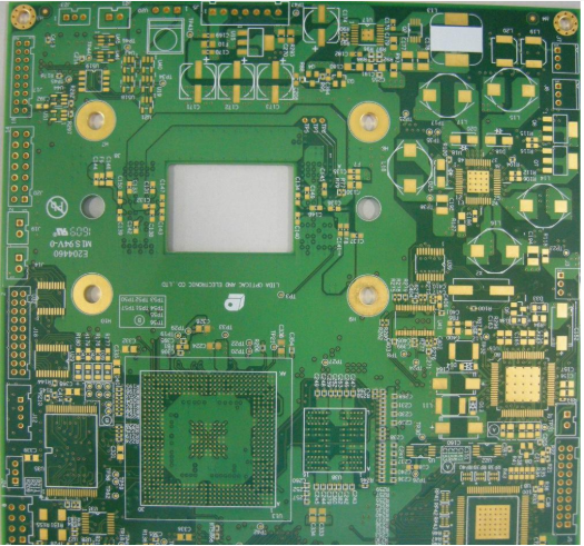
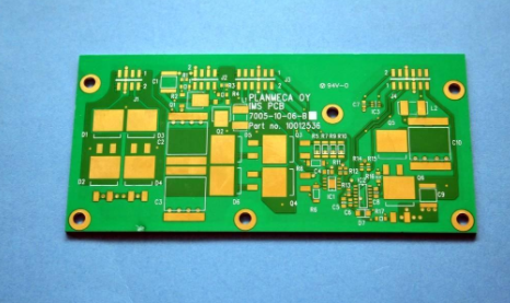
On the printed circuit board, the electrical connection of all components is carried out through pads. The pad is the most important basic unit in PCB design. According to different components and soldering processes, the pads in the printed circuit board can be divided into two types: non-via pads and via pads. Non-via pads are mainly used for soldering surface mount components, and via pads are mainly used for soldering pin-type components.
The choice of pad shape is related to the shape, size, layout, heating and force direction of the components and other factors. The designer needs to make a selection after comprehensive consideration according to the situation. In most PCB design tools, the system can provide designers with different types of pads such as round pads, rectangular pads and octagonal pads.
1. Round pad
In printed circuit boards, circular pads are the most commonly used pads. For via pads, the main dimensions of the circular pad are the aperture size and the pad size, and there is a proportional relationship between the pad size and the aperture size. For example, the pad size is generally twice the aperture size. Non-via circular pads are mainly used as test pads, positioning pads and reference pads, etc. The main size is the pad size.

2. Rectangular pad
Rectangular pads include square pads and rectangular pads. The square pad is mainly used to identify the first pin used to install components on the printed circuit board. Rectangular pads are mainly used as pin pads for surface mount components. The size of the pad is related to the size of the corresponding component pin, and the pad size of different components is different. For the specific dimensions of some component pads, please refer to section 1.3.
3. Octagonal pad
Octagonal pads are relatively rarely used in printed circuit boards, and they are mainly set to meet the requirements of printed circuit board wiring and pad soldering performance at the same time.
4. Special-shaped pad
In the PCB design process, designers can also use some special-shaped pads according to the specific requirements of the design. For example, for some pads with large heat generation, large force, large current, etc., they can be designed into a teardrop shape.
Pad size
The size of the pad has a great influence on the manufacturability and life of SMT products. There are many factors that affect the size of the pad. When designing the pad size, the range and tolerance of the component size, the need for the size of the solder joint, the accuracy, stability and process capabilities of the substrate (such as positioning and placement accuracy) should be considered when designing the pad size. The size of the pad is specifically determined by factors such as the shape and size of the components, the type and quality of the substrate, the capacity of the assembly equipment, the type and capacity of the process used, and the required quality level or standard.
The size of the designed pad, including the size of the pad itself, the size of the solder mask or the solder mask frame, the design needs to consider the footprint of the component, the wiring under the component and the dispensing (in the wave soldering process) Process requirements such as dummy pads or wiring.
As the current design of the pad size cannot find a specific and effective comprehensive mathematical formula, so users must also cooperate with calculations and experiments to optimize their own specifications, and can not just use other people's specifications or calculated results. Users should establish their own design files and develop a set of size specifications suitable for their actual conditions.
Users need to understand many aspects of information when designing pads, including the following parts.
1. Although there are international specifications for the packaging and thermal characteristics of components, the specifications differ greatly in some respects for different countries, different regions and different manufacturers. Therefore, the selection of components must be restricted or the design specifications must be divided into levels.
2. You need to have a detailed understanding of the quality of the PCB substrate(such as size and temperature stability), materials, process capabilities of mimeographs, and relative suppliers, and you need to organize and establish your own substrate specifications.
3. Need to understand the product manufacturing process and equipment capabilities, such as the size range of substrate processing, placement accuracy, screen printing accuracy, dispensing process, etc. Understanding this aspect will be of great help to the design of the pad.