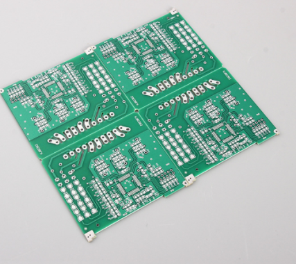
PCB circuit board production must have test points
However, in mass-produced factories, there is no way for you to use an electric meter to slowly measure whether each resistance, capacitance, inductance, and even IC circuits on each board are correct, so there is the so-called ICT (In -Circuit-Test) The emergence of automated test machines, which use multiple probes (generally called "Bed-Of-Nails" fixtures) to simultaneously contact all the parts on the board that need to be measured. Then, the characteristics of these electronic parts are measured in a sequence-based, parallel-based manner through programming. Usually, all parts of the general board can be tested in about 1 to 2 minutes, depending on the number of parts on the circuit board. It is determined that the more parts, the longer the time.
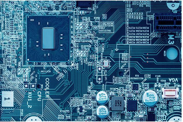
But if these probes directly touch the electronic parts on the board or its solder feet, it is likely to crush some electronic parts, but it is counterproductive, so there are test points, and a pair of circles are drawn at the two ends of the parts. There are no solder masks on the small shaped dots, so that the test probe can touch these small dots instead of directly touching the electronic parts to be measured.
In the early days when there were traditional plug-ins (DIP) on the circuit board, the solder feet of the parts were indeed used as test points, because the solder feet of the traditional parts were strong enough that they were not afraid of needle sticks, but there were often probes. The misjudgment of poor contact occurs, because after general electronic parts undergo wave soldering or SMT tin, a residual film of solder paste flux is usually formed on the surface of the solder, and the resistance of this film is It is very high, which often causes poor contact of the probe. Therefore, testing operators on the production line were often seen at that time, often holding an air spray gun to blow desperately, or using alcohol to wipe these places that needed to be tested.

Why should there be test points when PCB circuit board are produced
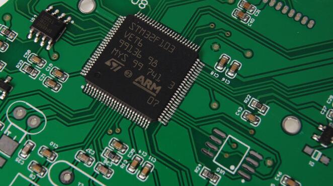
In fact, the test points after wave soldering will also have the problem of poor probe contact. Later, after the popularity of SMT, the misjudgment of the test was greatly improved, and the application of test points was also given a great deal of responsibility, because the parts of SMT are usually very fragile and cannot withstand the direct contact pressure of the test probe. Use test points. This eliminates the need for the probe to directly contact the parts and their solder feet, which not only protects the parts from damage, but also indirectly greatly improves the reliability of the test, because there are fewer misjudgments.
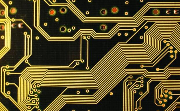
However, with the evolution of technology, the size of the circuit board has become smaller and smaller. It is already a bit difficult to squeeze so many electronic parts on the small circuit board. Therefore, the problem of the test point occupying the circuit board space is often A tug of war between the design end and the manufacturing end. The appearance of the test point is usually round, because the probe is also round, which is easier to produce, and it is easier to bring the adjacent probes closer, so that the needle density of the needle bed can be increased.
Using a needle bed for circuit testing has some inherent limitations on the mechanism, for example: the minimum diameter of the probe has a certain limit, and needles with too small diameter are easy to break and damage.
The distance between the needles is also limited, because each needle must come out of a hole, and the back end of each needle must be soldered with a flat cable. If the adjacent holes are too small, except for the gap between the needles There is the problem of contact short circuit, and the interference of the flat cable is also a big problem.
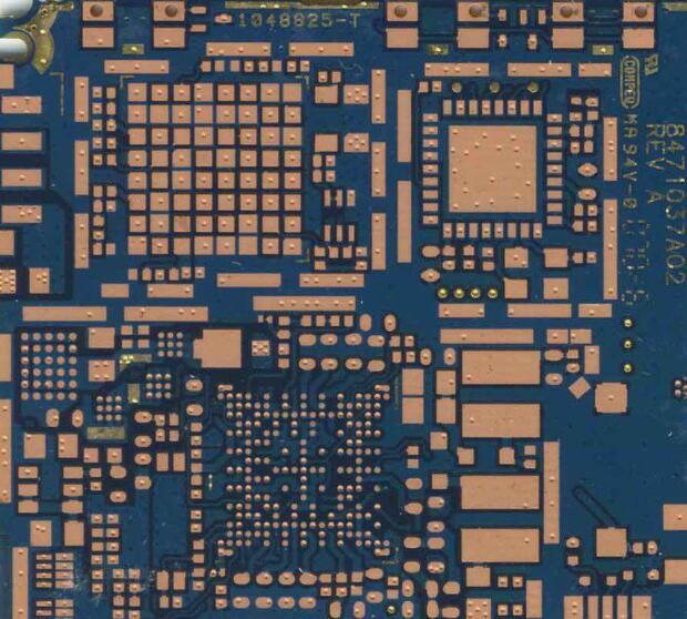
Some high parts cannot be implanted with needles. If the probe is too close to the high part, there is a risk of collision with the high part and cause damage. In addition, because of the high part, it is usually necessary to make holes in the needle bed of the test fixture to avoid it, which indirectly makes it impossible to implant the needle. Test points for all parts that are increasingly difficult to accommodate on the circuit board.
As PCB boards are getting smaller and smaller, the number of test points has been repeatedly discussed. Now there are some methods to reduce test points, such as Net test, Test Jet, Boundary Scan, JTAG... etc.; there are also other tests. The method intends to replace the original bed of needle tests, such as AOI and X-Ray, but it seems that each test cannot replace ICT 100%.