When talking about printed circuit board, novices often confuse "PCB schematics" and "PCB design files", but in fact they refer to different things. Understanding the differences between them is the key to successfully manufacturing PCBs, so in order to let beginners do this better, this article will break down the key differences between PCB schematics and PCB design.
What is a PCB printed circuit board
Before entering the difference between schematic and design, what you need to understand is, what is a PCB?
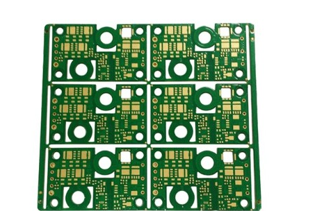
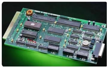
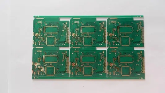
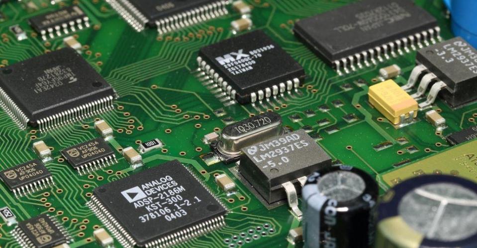
There are basically printed circuit board inside electronic equipment, also known as printed circuit board. This green circuit board made of precious metal connects all the electrical
Therefore, the design goals of PCB also have the following points: to properly fix various packaged components on the circuit board, and to be able to connect the signal of each pin of these devices (through the pad); PCB processing is Based on the Gerber file provided by the engineer to turn the design into an actual circuit board (bare board without components installed), there are many well-known PCB processing factories in China
components, and make it run normally. Without PCB, electronic equipment will not work.
PCB schematic and PCB design
PCB schematic is a simple two-dimensional circuit design that shows the functionality and connectivity between different components. The PCB design is a three-dimensional layout, and the position of the components is marked after the circuit is guaranteed to work normally.
Therefore, the PCB schematic is the first part of designing a printed circuit board. This is a graphical representation that uses agreed symbols to describe circuit connections, whether in written form or in data form. It also prompts the components to be used and how they are connected.
As the name suggests, the PCB schematic is a plan and a blueprint. It does not indicate where the components will be specifically placed. Rather, the schematic outlines how the PCB will ultimately achieve connectivity and constitutes a key part of the planning process.
After the blueprint is completed, the next step is the PCB design. The design is the layout or physical representation of the PCB schematic, including the layout of copper traces and holes. The PCB design shows the location of the above components and their connection to copper.
PCB design is a stage related to performance. Engineers built real components on the basis of PCB design so that they can test whether the equipment is working properly. As we mentioned earlier, anyone should be able to understand the PCB schematic, but it is not easy to understand its function by looking at the prototype.
After these two stages have been completed, and you are satisfied with the performance of the PCB, you need to implement it through the manufacturer.

PCB printed circuit board prototype schematic elements
After roughly understanding the difference between the two, let us take a closer look at the elements of the PCB schematic. As we mentioned, all connections are visible, but there are some caveats to keep in mind:
In order to be able to see the connections clearly, they are not created to scale; in the PCB design, they may be very close to each other
Some connections may cross each other, which is actually impossible
Some links may be on the opposite side of the layout, with a mark indicating that they are linked
This PCB "blueprint" can use one page, two pages or even a few pages to describe all the content that needs to be included in the design
The last thing to note is that more complex schematics can be grouped by function to improve readability. Arranging the connection in this way will not happen in the next stage, and the schematic diagram usually does not match the final design of the 3D model.
PCB printed circuit board prototype design elements
Now is the time to delve deeper into the elements of the PCB design file. At this stage, we transitioned from written blueprints to physical representations constructed using laminate or ceramic materials. When a particularly compact space is required, some more complex applications require the use of flexible PCBs.
The content of the PCB design file follows the blueprint established by the schematic flow, but, as mentioned before, the two are very different in appearance. We have discussed PCB schematics, but what differences can be observed in the design files?
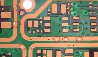
When we talk about PCB design files, we are talking about a 3D model, which includes printed circuit boards and design files. They can be single layer or multiple layers, although two layers are most common. We can observe some differences between PCB schematics and PCB design files:
All components are of correct size and position
If two points should not be connected, they must be detoured or switched to another PCB layer to avoid crossing each other on the same layer
In addition, as we briefly talked about, PCB design pays more attention to actual performance, because this is to some extent the verification phase of the final product. At this point, the practicality of the design must actually work comes into play, and the physical requirements of the printed circuit board must be considered. Some of these include:
How does the spacing of the components allow sufficient heat distribution
there are connectors on the edge
Regarding current and heat issues, how thick the various traces must be
Due to physical limitations and requirements means that the PCB design file usually looks very different from the design on the schematic, so the design file includes a screen printing layer. The silk screen layer indicates letters, numbers and symbols to help engineers assemble and use the board.
It is required to work as planned after all components are assembled on the printed circuit board. If not, you need to redraw.
Printed circuit board conclusion
Although PCB schematics and PCB design files are often confused, in fact, making PCB schematics and PCB design refer to two separate processes when creating a printed circuit board. The PCB schematic diagram that can draw the process flow must be created first, and then the PCB design can be carried out, and the PCB design is an important part of determining the performance and integrity of the PCB.