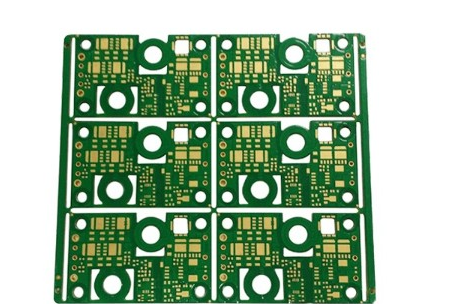
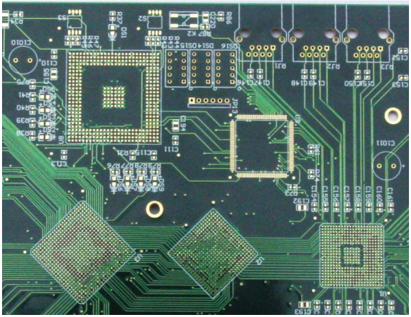
The high-precision printed circuit refers to the use of fine line width/spacing, micro holes, narrow ring width (or no ring width), and buried and blind holes to achieve high density. And high precision means that the result of "fine, small, narrow, thin" will inevitably lead to high precision requirements. Take the line width as an example: O.20mm line width, O.D. is produced according to regulations. 16~0.24mm is qualified, and its error is (O. 20 ± 0.04) mm; and O. For a line width of 10mm, the error is (0.10±0.02)mm. Obviously, the accuracy of the latter is increased by a factor of 1, and so on is not difficult to understand, so the high-precision requirements will not be discussed separately. But it is an outstanding problem in production technology.

(1) Fine wire technology In the future, the high and fine wire width/spacing will be increased from 0.20mm-O. Only 13mm-0.08mm-0.005mm can meet the requirements of SMT and Multichip Package (MCP). Therefore, the following technology is required.
1. Using thin or ultra-thin copper foil (<18um) substrate and fine surface treatment technology.
2. Using thinner dry film and wet filming process, thin and good quality dry film can reduce line width distortion and defects. Wet film can fill small air gaps, increase interface adhesion, and improve wire integrity and accuracy.
3. Using parallel light exposure technology. Since parallel light exposure can overcome the influence of the line width variation caused by the oblique rays of the "point" light source, it is possible to obtain fine wires with precise line width dimensions and smooth edges. However, the parallel exposure equipment is expensive, the investment is high, and it is required to work in a high cleanliness environment.
4. Electrodeposited Photoresist (Electro-deposited Photoresist, ED) is used. Its thickness can be controlled in the range of 5-30/um, which can produce more perfect fine wires. It is especially suitable for narrow ring width, no ring width and full plate electroplating. There are currently more than a dozen ED production lines in the world.
5. Using automatic optical inspection technology (Automatic Optic Inspection, AOI). This technology has become an indispensable means of detection in the production of fine wires, and is rapidly being promoted, applied and developed.
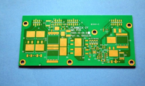
(2) Microporous technology The functional holes of the printed circuit board used for surface mounting are mainly used for electrical interconnection, which makes the application of microporous technology more important. The use of conventional drill materials and CNC drilling machines to produce tiny holes has many failures and high costs. Therefore, the high-density of printed boards is mostly focused on the refinement of wires and pads. Although great achievements have been made, its potential is limited. To further improve the densification (such as wires less than 0.08mm), the cost is urgent. Therefore, it turns to use micropores to improve the densification.
In recent years, numerical control drilling machines and micro-drill technology have made breakthrough progress, so micro-hole technology has developed rapidly. This is the main outstanding characteristic in the current printed board production. In the future, the micro-hole forming technology will mainly rely on advanced CNC drilling machines and excellent micro-heads, and the small holes formed by laser technology are still inferior to those formed by CNC drilling machines from the viewpoint of cost and hole quality.
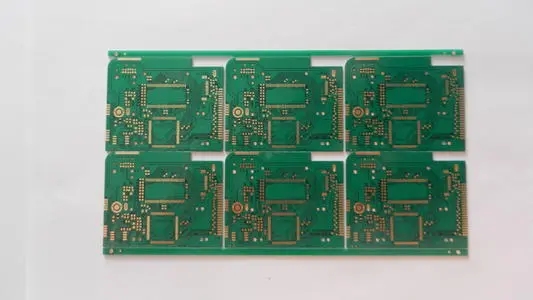
1. Buried, blind, and through-hole technology The combination of buried, blind, and through-hole technology is also an important way to increase the density of printed circuits. Generally, the buried and blind holes are all tiny holes. In addition to increasing the number of wiring on the board, the buried and blind holes are interconnected by the "nearest" inner layer, which greatly reduces the number of through holes formed, and the setting of the isolation disk will also be greatly reduced. Reduce, thereby increasing the number of effective wiring and inter-layer interconnection in the board, and improving the high density of interconnection. Therefore, the multi-layer board with the combination of buried, blind, and through-holes has at least three times higher interconnection density than the conventional full-through-hole structure under the same size and number of layers. If the buried, blind, and The size of the printed board combined with through holes will be greatly reduced or the number of layers will be significantly reduced. Therefore, in high-density surface-mounted printed boards, buried and blind hole technologies have been increasingly used, not only in surface-mounted printed boards in large computers, communication equipment, etc., but also in civil and industrial applications. It has also been widely used in the field, even in some thin boards, such as various thin six-layer boards such as PCMCIA, Smard, and IC cards.
Printed circuit boards with buried and blind hole structures are generally completed by "sub-board" production methods, which means that they must be completed through multiple pressing, drilling, and hole plating, so precise positioning is very important .
2. Numerical control drilling machine At present, the technology of numerical control drilling machine has made new breakthroughs and progress. And formed a new generation of CNC drilling machine characterized by drilling tiny holes. The efficiency of drilling small holes (less than 0.50mm) of the micro-hole drilling machine is 1 times higher than that of the conventional CNC drilling machine, with fewer failures, and the rotation speed is 11-15r/min; it can be drilled at 0. 1~0.2mm micro-holes, using high-quality small drills with high cobalt content, three plates (1.6mm/block) can be stacked for drilling. When the drill bit is broken, it can automatically stop and report the position, automatically replace the drill bit and check the diameter (the tool library can hold hundreds of pieces), and can automatically control the constant distance between the drill tip and the cover and the drilling depth, so blind holes can be drilled, It will not damage the countertop. The surface of the CNC drilling machine adopts air cushion and magnetic suspension type, which can move faster, lighter, and more accurately without scratching the surface. Such drilling machines are currently in demand, such as the Mega 4600 from Prurite in Italy, the ExcelIon 2000 series in the United States, and new generation products from Switzerland and Germany.
3. There are indeed many problems with laser drilling conventional CNC drilling machines and drill bits to drill tiny holes. It has hindered the progress of micro-hole technology, so laser ablation has received attention, research and application. But there is a fatal shortcoming, that is, the formation of a horn hole, which becomes more serious as the plate thickness increases. Coupled with high-temperature ablation pollution (especially multi-layer boards), the life and maintenance of the light source, the repeatability of the corrosion holes, and the cost, etc., the promotion and application of micro-holes in the production of printed boards has been limited. However, laser ablation is still used in thin and high-density microporous plates, especially in MCM-L's high-density interconnect (HDI) technology, such as M. C. The polyester film etching hole in Ms and the metal deposition (sputtering technology) are combined in high-density interconnection. The formation of buried vias in high-density interconnection multilayer boards with buried and blind via structures can also be applied. However, due to the development and technological breakthroughs of CNC drilling machines and micro-drills, they were quickly promoted and applied. Therefore, the application of laser drilling in surface mount printed boards cannot form a dominant position. But it still has a place in a certain field.
The above is the introduction of high-density PCB production technology. Ipcb also provides PCB manufacturers and PCB manufacturing technology.