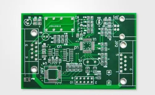
PCB board layout knowledge

1 When a high-speed optical module is included, the layout of the optical port transceiver circuit is prioritized.
2 The layout of the power supply section ensures that the input and output lines are smooth and do not cross.
3 When the single board supplies power to the subboard, place the corresponding filter circuit near the power outlet of the single board and the power inlet of the subboard.
4 The layout takes into account the smoothness of the overall wiring, and the main data flow is reasonable.
5 Adjust the pin assignments of devices such as exclusion, FPGA, EPLD, bus driver, etc. according to the layout results to optimize the layout.
6 The layout considers the appropriate increase of the space at the dense traces to avoid the situation that cannot be routed.
7 If special materials, special devices (such as 0.5mmBGA, etc.), and special processes are adopted, the delivery period and processability have been fully considered, and confirmed by PCB manufacturers and process personnel.
8 The pin corresponding relationship of the sub-board connector has been confirmed to prevent the direction and orientation of the sub-board connector from being reversed.
9 If there are ICT test requirements, consider the feasibility of adding ICT test points during layout to avoid difficulty in adding test points during the wiring phase.
10 After the layout is completed, a 1:1 assembly drawing has been provided for the project personnel to check whether the device package selection is correct against the device entity.
11 At the opening of the window, the inner plane has been considered to be retracted, and a suitable wiring prohibition area has been set.
Circuit board layout EMC tips
1 The interface components are placed close to the edge of the board, and appropriate EMC protection measures have been taken (such as shielding shells, hollowing out of the power supply ground, etc.) to improve the EMC capability of the design.
2 In order to avoid electromagnetic interference between devices on the welding surface of the single board and adjacent single boards, no sensitive devices and strong radiation devices should be placed on the welding surface of the single board.
3 Inductive devices that are prone to magnetic field coupling, such as inductors, relays, and transformers, should not be placed close to each other. When there are multiple inductance coils, the direction is vertical and they are not coupled.
4 The distance from the shielding body and the shielding shell to the shielding body and shielding shell is more than 500 mils for the devices with high transmitting power or particularly sensitive (such as crystal oscillators, crystals, etc.).
5 The protection circuit is placed near the interface circuit, following the principle of first protection and then filtering.
6 A 0.1uF capacitor is placed near the reset line of the reset switch to keep the reset device and reset signal away from other strong devices and signals.
The above is an introduction to the small knowledge of circuit board layout in PCB design. Ipcb is also provided to PCB manufacturers and PCB manufacturing technology.