Physical partitioning mainly involves issues such as component layout, orientation, and shielding; electrical partitioning can continue to be decomposed into partitions for power distribution, RF wiring, sensitive circuits and signals, and grounding.

1 We discuss the issue of physical partitioning. Component layout is the key to achieving a good RF design. The most effective technique is to first fix the components on the RF path and adjust their orientation to minimize the length of the RF path, keep the input away from the output, and as far as possible Ground separation of high-power circuits and low-power circuits.
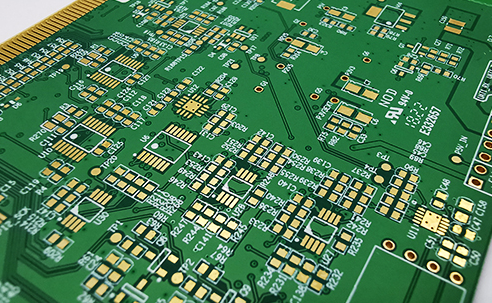
The most effective PCB board stacking method is to arrange the main ground plane (main ground) on the second layer below the surface layer, and route the RF lines on the surface layer as much as possible. Minimizing the size of the vias on the RF path can not only reduce the path inductance, but also reduce the virtual solder joints on the main ground and reduce the chance of RF energy leaking to other areas in the laminate. In physical space, linear circuits like multi-stage amplifiers are usually sufficient to isolate multiple RF zones from each other, but duplexers, mixers, and intermediate frequency amplifiers/mixers always have multiple RF/IFs. The signals interfere with each other, so care must be taken to minimize this effect.
2 The RF and IF traces should be crossed as much as possible, and a ground should be placed between them as much as possible. The correct RF path is very important to the performance of the entire PCB board, which is why the component layout usually accounts for most of the time in the mobile phone PCB board design. In the mobile phone PCB board design, usually the low-noise amplifier circuit can be placed on one side of the PCB board, and the high-power amplifier is placed on the other side, and finally they are connected to the RF end and baseband processing on the same side through a duplexer. On the antenna at the end of the device. Some tricks are needed to ensure that the straight through holes do not transfer RF energy from one side of the board to the other. A common technique is to use blind holes on both sides. The adverse effects of the straight-through holes can be minimized by arranging the straight-through holes in areas that are free from RF interference on both sides of the PCB board. Sometimes it is impossible to ensure sufficient isolation between multiple circuit blocks. In this case, it is necessary to consider the use of a metal shield to shield the RF energy in the RF area. The metal shield must be soldered to the ground and must be kept with the components. A proper distance, so it needs to take up valuable PCB board space. It is very important to ensure the integrity of the shielding cover as much as possible. The digital signal lines entering the metal shielding cover should go to the inner layer as much as possible, and it is best that the PCB layer below the wiring layer is the ground layer. The RF signal line can go out from the small gap at the bottom of the metal shield and the wiring layer at the ground gap, but as much ground as possible around the gap, and the ground on different layers can be connected together through multiple vias. .
3 Proper and effective chip power decoupling is also very important. Many RF chips with integrated linear circuits are very sensitive to power noise. Usually, each chip needs to use up to four capacitors and an isolation inductor to ensure that all power noise is filtered out. An integrated circuit or amplifier often has an open-drain output, so a pull-up inductor is required to provide a high-impedance RF load and a low-impedance DC power supply. The same principle applies to decoupling the power supply at this inductor side. Some chips require multiple power supplies to work, so you may need two or three sets of capacitors and inductors to decouple them separately. The inductors are rarely close together in parallel, because this will form an air-core transformer and induce interference with each other. Signals, so the distance between them must be at least equal to the height of one of the devices, or arranged at right angles to minimize their mutual inductance.
4 The principle of electrical zoning is roughly the same as that of physical zoning, but it also contains some other factors. Some parts of the mobile phone use different working voltages and are controlled by software to extend the battery life. This means that mobile phones need to run multiple power sources, and this brings more problems to isolation. The power is usually introduced from the connector, and is immediately decoupled to filter out any noise from the outside of the circuit board, and then distributed after passing through a set of switches or regulators. The DC current of most circuits on the mobile phone PCB board is quite small, so the trace width is usually not a problem. However, a large current line as wide as possible must be routed separately for the power supply of the high-power amplifier to minimize the transmission voltage drop. . In order to avoid too much current loss, multiple vias are needed to transfer current from one layer to another. In addition, if it cannot be sufficiently decoupled at the power supply pin of the high-power amplifier, high-power noise will radiate to the entire board and cause various problems. The grounding of high-power amplifiers is critical, and it is often necessary to design a metal shield for it. In most cases, it is also critical to ensure that the RF output is far away from the RF input. This also applies to amplifiers, buffers and filters. In the worst case, if the output of the amplifier and buffer is fed back to their input with appropriate phase and amplitude, then they may have self-oscillation. In the best case, they will be able to work stably under any temperature and voltage conditions. In fact, they may become unstable and add noise and intermodulation signals to the RF signal. If the RF signal line has to be looped from the input end of the filter back to the output end, this may seriously damage the bandpass characteristics of the filter. In order to get a good isolation between the input and the output, a ground must be laid around the filter first, and then a ground must be laid in the lower layer area of the filter and connected to the main ground surrounding the filter. It is also a good way to keep the signal lines that need to pass through the filter as far away as possible from the filter pins.
In addition, the grounding of various places on the whole board must be very careful, otherwise a coupling channel will be introduced. Sometimes you can choose to take single-ended or balanced RF signal lines. The principles of cross-interference and EMC/EMI are also applicable here. Balanced RF signal lines can reduce noise and cross-interference if they are routed correctly, but their impedance is usually high, and a reasonable line width must be maintained to obtain a matching signal source, trace and load impedance. The actual wiring may be There will be some difficulties. The buffer can be used to improve the isolation effect, because it can divide the same signal into two parts and used to drive different circuits, especially the local oscillator may need a buffer to drive multiple mixers. When the mixer reaches the common mode isolation state at the RF frequency, it will not work properly. The buffer can well isolate the impedance changes at different frequencies, so that the circuits will not interfere with each other. Buffers are very helpful to the design. They can follow the circuit that needs to be driven, so that the high-power output traces are very short. Because the input signal level of the buffer is relatively low, they are not easy to interfere with other on the board. The circuit is causing interference. Voltage-controlled oscillators (VCOs) can convert varying voltages into varying frequencies. This feature is used for high-speed channel switching, but they also convert trace noise on the control voltage into tiny frequency changes, which gives The RF signal adds noise.
5 To ensure that noise is not increased, the following aspects must be considered: First, the expected bandwidth of the control line may range from DC to 2MHz, and it is almost impossible to remove such wide-band noise through filtering; secondly, the VCO control line It is usually part of a feedback loop that controls the frequency. It may introduce noise in many places, so the VCO control line must be handled very carefully. Make sure that the ground below the RF trace is solid, and all components are firmly connected to the main ground and isolated from other traces that may cause noise. In addition, it is necessary to ensure that the power supply of the VCO has been sufficiently decoupled. Since the RF output of the VCO is often a relatively high level, the VCO output signal can easily interfere with other circuits, so special attention must be paid to the VCO. In fact, VCO is often placed at the end of the RF area, and sometimes it needs a metal shield. The resonant circuit (one for the transmitter and the other for the receiver) is related to the VCO, but it also has its own characteristics. Simply put, the resonant circuit is a parallel resonant circuit with capacitive diodes, which helps to set the VCO operating frequency and modulate voice or data to the RF signal. All VCO design principles also apply to resonant circuits. Because the resonant circuit contains a considerable number of components, has a wide distribution area on the board, and usually runs at a very high RF frequency, the resonant circuit is usually very sensitive to noise. Signals are usually arranged on adjacent pins of the chip, but these signal pins need to work with relatively large inductors and capacitors, which in turn requires these inductors and capacitors to be located very close and connected back On a control loop that is sensitive to noise. It is not easy to do this.
Automatic gain control (AGC) amplifier is also a problem-prone place, whether it is a transmitting or receiving circuit will have an AGC amplifier. AGC amplifiers can usually effectively filter out noise, but because mobile phones have the ability to deal with the rapid changes in the intensity of transmitted and received signals, the AGC circuit is required to have a fairly wide bandwidth, which makes it easy to introduce AGC amplifiers on some key circuits noise. Designing AGC circuits must comply with good analog circuit design techniques, which are related to the short op amp input pins and short feedback paths, both of which must be far away from RF, IF, or high-speed digital signal traces. Similarly, good grounding is also essential, and the chip's power supply must be well decoupled. If it is necessary to run a long wire at the input or output end, it is best to go at the output end. Usually, the impedance of the output end is much lower and it is not easy to induce noise. Generally, the higher the signal level, the easier it is to introduce noise into other circuits. In all PCB designs, it is a general principle to keep digital circuits away from analog circuits as much as possible, and it also applies to RF PCB design. Common analog ground and ground for shielding and separating signal lines are usually equally important. Therefore, in the early stages of design, careful planning, well-considered component layout, and thorough layout evaluation are all very important, and RF circuits should also be used Keep away from analog lines and some very critical digital signals. All RF traces, pads and components should be filled with grounded copper as much as possible and connected to the main ground as much as possible. If the RF trace must pass through the signal line, try to route a layer of ground connected to the main ground along the RF trace between them. If it is not possible, make sure that they are crossed, which can minimize capacitive coupling. At the same time, place as much ground as possible around each RF trace and connect them to the main ground. In addition, minimizing the distance between parallel RF traces can minimize inductive coupling. When a solid ground plane is placed directly on the first layer below the surface, the isolation effect is best, although other methods of designing with care will also work. On each layer of the PCB board, place as many grounds as possible and connect them to the main ground. Place the traces as close together as possible to increase the number of plots of the internal signal layer and power distribution layer, and adjust the traces appropriately so that you can arrange the ground connection vias to the isolated plots on the surface. Free ground should be avoided on the various layers of the PCB because they can pick up or inject noise like a small antenna. In most cases, if you can't connect them to the main land, then you'd better remove them.