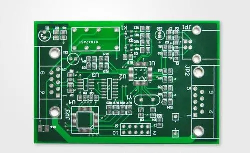
In PCB Layout design, in addition to considering the problem of its own wiring, some hidden problems should also be considered. These problems are inconspicuous when designing, but it is very troublesome to solve them. This is the problem of circuit interference.

In the PCB design process, only knowing some design basics can only solve simple and low-frequency PCB design problems, but it is much more difficult for complex and high-frequency PCB design. It often takes many times the time to solve the problems that are not considered carefully by the design, and it may even be redesigned. For this reason, the following problems should be solved in the design of the PCB:
Thermal interference and resistance of advanced PCB design
The components have a certain degree of heat during operation, especially the heat emitted by the more powerful devices will interfere with the surrounding temperature-sensitive devices. If the thermal interference is not well suppressed, the electrical power of the entire circuit Performance will change.
Common impedance and suppression of advanced PCB design
Common resistance interference is caused by a large number of ground wires on the PCB board. When two or more loops share a section of ground wire, different loop currents will produce a certain voltage drop on the shared ground wire. This voltage drop will affect the circuit performance when amplified; when the current frequency is very high, it will produce The circuit is disturbed by the large inductance.
Electromagnetic interference and suppression of advanced PCB design
Electromagnetic interference is the interference caused by electromagnetic effects. As the components and wiring on the PCB are getting denser, electromagnetic interference will occur if the design is improper.
Width and spacing of printed wires in PCB design rules
The width and spacing of printed wires, generally the minimum width of wires is 0.5-0.8mm, and the spacing is not less than 1mm.
(1) The minimum width of the printed wire: It is mainly determined by the adhesion strength between the wire and the insulating substrate and the current value flowing through them. Due to the large current flow, the power and ground wires of PCB should be appropriately widened during design, generally not less than 1mm. For PCBs with low mounting density, the width of printed conductors is best not less than 0.5mm. Hand-made boards should not be Less than 0.8mm.
(2) Printed conductor spacing: determined by the safe working voltage between them. The peak voltage between adjacent wires, the quality of the substrate, the surface coating, and the capacitive coupling parameters all affect the safe working voltage of the printed wires.
PCB design rules for printed wiring wiring
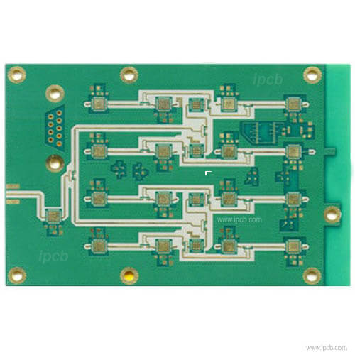
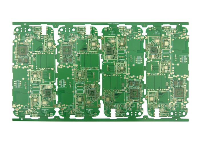
Wiring refers to the placement of the direction and shape of printed wires. It is the most critical step in PCB design, and it is the step with the largest workload. PCB wiring includes single-sided wiring, double-sided wiring and multi-layer wiring; there are also two ways of wiring: automatic wiring and manual wiring.
In PCB design, in order to obtain a satisfactory wiring effect, the following basic principles should be followed:
1) The direction of the printed line-take it as straight as possible, preferably short, and don't go too far.
2) The bending of the printed line-the routing is smooth and natural, and the connection is rounded, avoiding right angles.
3) Printed wires on the double-sided board-the wires on both sides should be avoided to be parallel to each other; the printed wires used as the input and output of the circuit should be avoided as much as possible, and it is better to add a grounding wire between these wires.
4) The printed wire is used as a ground wire-keep as much copper foil as a common ground wire as much as possible and arrange it on the edge of the PCB.
5) The use of large-area copper foil-it is best to hollow out into a grid during use, which is beneficial to eliminate the volatile gas generated by the heating of the adhesive between the copper foil and the substrate; when the wire width exceeds 3mm, a groove is left in the middle to facilitate welding.
The spacing and installation dimensions of components in PCB design rules
It is about the spacing between the elements and the size of the installation during the layout of the components in the PCB design.
(1) Pin spacing of components: Different components have different pin spacing. But for all kinds of components, the pin spacing is mostly: 100mil (English) integer multiples (1mil=l*10(-3 cubic)in=25.4*10(-6th power)m), 100mil is often regarded as 1 pitch. In the PCB design, the pin spacing of the components must be accurately clarified, because it determines the pad placement spacing. The most direct way to determine the pin spacing of non-standard devices is to use a vernier caliper to measure.
Pin spacing of common components a) DIP IC b) TO-92 type three pole tube c) 1/4w type resistor d) a trimming resistor
(2) The installation size of the components: the solder hole pitch is determined according to the pin pitch. It has soft size and hard size. The soft size is based on the components whose pins can be bent, so the design of the soldering pitch of this type of device is more flexible; while the hard size is based on the components whose pins cannot be bent, and the soldering pitch requirements are quite accurate. When designing the PCB, the solder hole spacing of the components can be determined by the calibration tool in the CAD software.
Arrangement of components in PCB design rules
The arrangement of the components on the PCB can be one of three arrangements: irregular, regular, and grid, or multiple at the same time.
(1) Irregular arrangement: The axis directions of the components are inconsistent with each other, which is convenient for the layout of printed wires, and has high plane utilization and small distribution parameters, which is especially beneficial for high-frequency circuits.
(2) Regular arrangement: The components are arranged in the same axial direction, and the layout is beautiful and neat, but the wiring is long and complicated, which is suitable for low-frequency circuits.
(3) Grid arrangement: each mounting hole in the grid arrangement is designed at the intersection of the square grid.
The layout of the components of the PCB layout design rules
The layout methods of the components of the PCB design rules include: component layout requirements, component layout principles, component layout order, and layout methods of commonly used components.
In PCB LAYOUT, when we use Protel, DXP, PADS, Protel DXP and other tools to draw the circuit board, we need to pay attention to the following aspects
(1) Component layout requirements: ensure circuit functions and performance indicators; meet the requirements of processability, testing, maintenance, etc.; components are arranged neatly, densely, and aesthetics.
(2) The principle of component layout: The arrangement direction should be as consistent as possible with the schematic diagram, and the wiring direction should be consistent with the wiring direction of the circuit diagram; there are 5-10mm gaps around the PCB that do not place the components; the layout of the components should be conducive to heating components Heat dissipation; At high frequency, the distribution parameters between components should be considered. Generally, the circuit should be arranged in parallel as much as possible; high and low voltages should be isolated. The isolation distance is related to the withstand voltage. For a single-sided PCB, each component pin occupies a unique pad, and the components cannot cross up and down, and a certain distance should be maintained between two adjacent components, and they should not be too small or touched.
(3) Layout order of components: place the components with a larger area first; integrate first and then separate; first main and then second, and place the main circuit first in the case of multiple integrated circuits.
(4) Layout method of common components: adjustable components should be placed on the printed circuit board for easy adjustment; components with a mass of more than 15g should use brackets, and high-power components should be installed on the chassis bottom plate of the whole machine. Sensitive components should be far away from heating components; for tubular components, they are generally placed horizontally, but when the PCB size is not large, they can be placed vertically. When placed vertically, the distance between the two pads is generally 0.1-0.2 in(1 in="25" .4*10 (-3 cubic) m); For integrated circuits, it is necessary to determine whether the orientation of the positioning slot is correct.