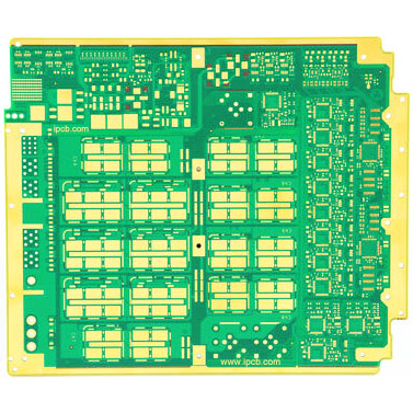
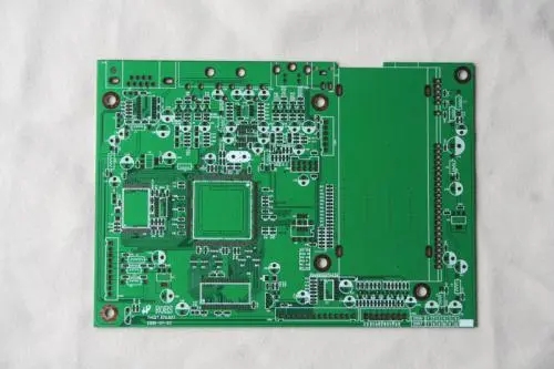
1. Straight board machine
Assuming that the mobile phone has a baseband chip, power management module, RAM, receiver, transmitter, VCO, PA, RF switch, RF connector, SIM card holder, USB, motor, battery connector, crystal oscillator, backup battery
Because the buttons and screen of the candy bar are generally on the same side of the motherboard, the baseband and RAM can be placed under the screen. At the same time, the extra space can be used to place the Bluetooth module.

Because the antenna is to be placed on the back, according to the principle of short RF signal lines, the RF components need to be placed on this side, close to the antenna->the far is the RF switch, PA (GSM PA and 3G PA need to be placed reasonably), VCO, then down, place the receiver and transmitter on the left and right. Place the PMIC and T-CARD at the bottom, which can be placed on the side of the surface.
19.2Mhz TCXO (temperature-compensated crystal oscillator) provides clock signals for receivers, transmitters, PMIC and Bluetooth. These wires need to be covered up, down, left and right.
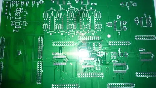
2. Clamshell machine
Clamshell machine buttons are generally placed directly on the motherboard (rather than through the card holder), and all chips need to be placed on one side. At this time, the baseband chip, RAM, and power management module should be placed as far away from the antenna as possible. The RF device is consistent with the requirements of the candy bar.
When Layout, the RF input and output signals should be as far away as possible. The minimum distance between RF signals should be twice the line width. The data signal lines and address signal lines between the baseband chip and RAM are generally routed on the second and third layers. over. The wiring of layer 2 and layer 3 needs to be crossed, and the wiring can be appropriately wound to achieve this purpose. In order to ensure that the impedance of the radio frequency line is 50 ohm, the surface radio frequency line needs to be stripped of the surrounding ground, so as not to provide a return path, thereby affecting the size of the impedance. The distance between the same layer of 50ohm line and the ground is at least 2 times the line distance (if the surface line is too thick, keep 10MIL)
At least one layer of ground must be kept intact. In addition, the grounds of the upper and lower layers that directly correspond to the strip line must be intact and no wiring is allowed!
There can only be RF connectot and matching capacitance and sensing parts under the antenna, otherwise it may seriously affect the wireless index.
The above is the introduction of mobile phone PCB Layout experience summary, Ipcb also provides PCB manufacturers and PCB manufacturing technology