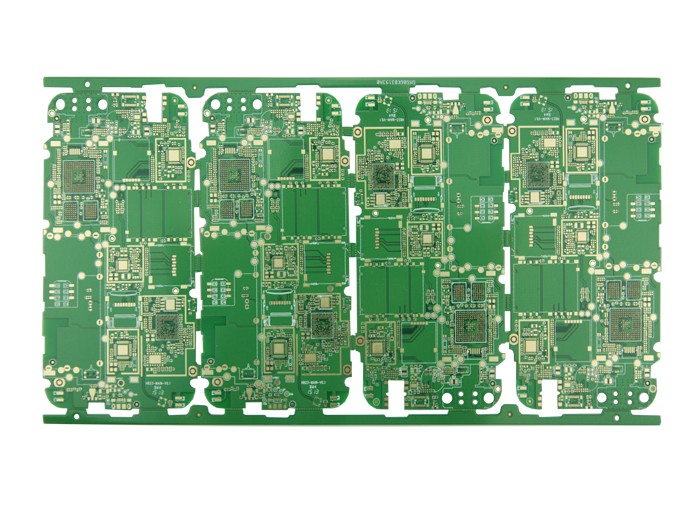
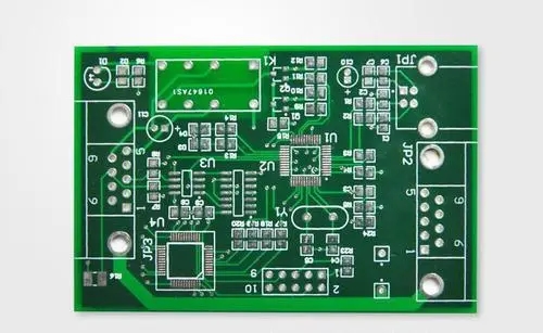
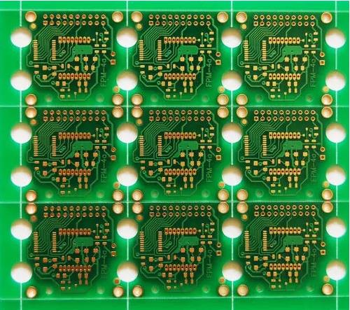
For electronic products, printed PCB circuit board design is a design process necessary for it to change from an electrical schematic diagram to a specific product. The rationality of its design is closely related to product production and product quality. For many people who are just engaged in electronic design For the people, they have less experience in this area. Although they have learned the printed circuit board design software, the printed PCB circuit boards they designed often have problems of this kind, and many electronic publications have few articles in this area. The author has been engaged in the work of printed circuit board design for many years, and I will share with you some experience in printed circuit board design, hoping to play a role in attracting new ideas. The author's printed circuit board design software was TANGO a few years ago, and now it uses PROTEL2.7 FOR WINDOWS.

Board layout:
The usual order of placing the components on the printed circuit board:
Place components in fixed positions that closely match the structure, such as power sockets, indicator lights, switches, connectors, etc. After these components are placed, use the LOCK function of the software to lock them so that they will not be moved by mistake in the future;
Place special components and large components on the circuit, such as heating components, transformers, ICs, etc.;
Place small devices. The distance between the components and the edge of the board: if possible, all components should be placed within 3mm from the edge of the board or at least greater than the board thickness. This is because the assembly line plug-in and wave soldering in mass production must be provided to the guide groove In order to prevent the defect of the edge part due to the shape processing, if there are too many components on the printed circuit board, if it is necessary to exceed the 3mm range, you can add a 3mm auxiliary edge to the edge of the board, and the auxiliary edge shall be V-shaped The groove can be broken by hand during production.
Isolation between high and low voltage: There are both high voltage and low voltage circuits on many printed circuit boards. The components of the high voltage circuit part and the low voltage part should be separated from each other. The isolation distance is related to the withstand voltage to be withstood. Normally At 2000kV, the distance between the board should be 2mm, and the distance should be increased in proportion to this. For example, if you want to withstand the 3000V withstand voltage test, the distance between the high and low voltage lines should be above 3.5mm. In many cases, it is to avoid Creepage, also slotting between the high and low voltage on the printed circuit board.
The wiring of the printed circuit board:
The layout of printed wires should be as short as possible, especially in high-frequency circuits; the bends of printed wires should be rounded, and right or sharp corners will affect electrical performance in high-frequency circuits and high wiring density. ; When the two panels are wired, the wires on both sides should be perpendicular, oblique, or bent to avoid parallel to each other to reduce parasitic coupling; printed wires used as the input and output of the circuit should be avoided as far as possible. In order to avoid feedback, it is best to add a ground wire between these wires.
Width of printed wire:
The width of the wire should be such that it can meet the electrical performance requirements and is convenient for production. Its minimum
The value depends on the magnitude of the current, but the minimum should not be less than 0.2mm. In the high-density, high-precision printed circuit, the wire width and spacing can generally be 0.3mm; the wire width should also consider its temperature rise in the case of large currents, Single-panel experiments show that when the thickness of the copper foil is 50μm, the wire width is 1~1.5mm, and the current is 2A, the temperature rise is very small. Therefore, the general selection of 1~1.5mm width wire may meet the design requirements without causing temperature rise ; The public ground wire of the printed wire should be as thick as possible. If possible, use a line larger than 2 to 3mm. This is particularly important in circuits with microprocessors, because when the ground wire is too thin, due to the current flowing The change of the ground potential, the unstable level of the microprocessor timing signal will degrade the noise margin; the 10-10 and 12-12 principles can be applied to the wiring between the IC pins of the DIP package, that is, when two pins are used. When two wires pass in between, the pad diameter can be set to 50mil, and the line width and line spacing are both 10mil. When only one wire passes between the two legs, the pad diameter can be set to 64mil, and the line width and line spacing are both 12mil.
Pitch of printed wires:
The distance between adjacent wires must be able to meet electrical safety requirements, and in order to facilitate operation and production, the distance should be as wide as possible. The minimum distance must be at least suitable for the withstand voltage. This voltage generally includes working voltage, additional fluctuating voltage, and peak voltage caused by other reasons. If the relevant technical conditions allow a certain degree of metal residue between the wires, the spacing will be reduced. Therefore, the designer should take this factor into consideration when considering the voltage. When the wiring density is low, the spacing of the signal lines can be appropriately increased, and the signal lines with high and low levels should be as short as possible and the spacing should be increased.
Shielding and grounding of printed wires:
The common ground wire of the printed wire should be arranged on the edge of the printed circuit board as far as possible. Keep as much copper foil as the ground wire on the printed circuit board. The shielding effect obtained in this way is better than that of a long ground wire. The transmission line characteristics and shielding effect will be improved, and the distributed capacitance will be reduced. . The common ground of the printed conductors is best to form a loop or a mesh. This is because when there are many integrated circuits on the same board, especially when there are more power-consuming components, the ground potential difference is generated due to the limitation of the pattern., Resulting in the reduction of noise tolerance, when it is made into a loop, the ground potential difference is reduced. In addition, the graphics of grounding and power supply should be as parallel as possible to the direction of data flow. This is the secret of enhancing the ability to suppress noise; multi-layer printed circuit boards can adopt several layers as shielding layers, and the power layer and ground layer are both visible. For the shielding layer, the ground layer and power layer are generally designed on the inner layer of the multilayer printed circuit board, and the signal wires are designed on the inner and outer layers.
Pad:
Pad diameter and inner hole size: The inner hole size of the pad must be considered from the component lead diameter and tolerance size, as well as the thickness of the tin-lined layer, the hole diameter tolerance, and the thickness of the hole metallization plating layer. The inner hole of the pad is generally not smaller than 0.6mm, because the hole less than 0.6mm is not easy to process when punching, usually the diameter of the metal pin plus 0.2mm is used as the diameter of the inner hole of the pad. For example, when the diameter of the metal pin of the resistor is 0.5mm, the pad The inner hole diameter corresponds to 0.7mm, and the pad diameter depends on the inner hole diameter, as shown in the following table:
Hole diameter
0.4
0.5
0.6
0.8
1.0
1.2
1.6
2.0
Pad diameter
1.5
1.5
2
2.5
3.0
3.5
4
1. When the diameter of the pad is 1.5mm, in order to increase the stripping strength of the pad, a length of not less than 1.5mm, a width of 1.5mm and an oblong pad can be used. This kind of pad is the most common in integrated circuit pin pads. .
2. For pad diameters beyond the range of the above table, the following formula can be used to select:
Hole diameter less than 0.4mm: D/d=0.5~3
Holes with a diameter greater than 2mm: D/d=1.5~2
In the formula: (D-pad diameter, d-inner hole diameter)
Other notes about pads:
The distance between the edge of the inner hole of the pad and the edge of the printed board should be greater than 1mm, which can avoid the defects of the pad during processing.
The opening of the pad: some devices are repaired after wave soldering, but after the wave soldering, the inner hole of the pad is sealed by tin, so that the device cannot be inserted. The solution is to solder it during the printed board processing. Make a small opening so that the inner hole will not be sealed during wave soldering, and it will not affect normal soldering.
Pad fill teardrop: When the trace connected to the pad is thin, the connection between the pad and the trace should be designed into a drop shape. The advantage of this is that the pad is not easy to peel, but the trace is The pad is not easily broken. Adjacent pads should avoid sharp angles or large-area copper foils. Acute angles will cause difficulty in wave soldering, and there is a risk of bridging. Large-area copper foils will not be easy to solder due to excessive heat dissipation.
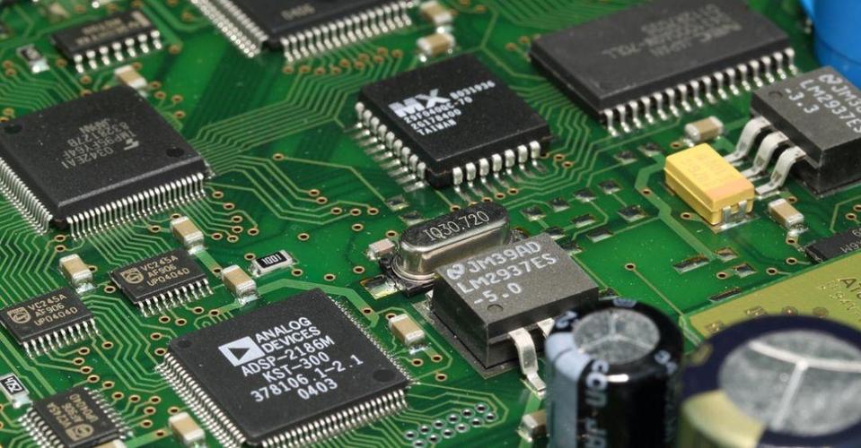
Large-area copper coating: The large-area copper coating on the printed circuit board is often used for two functions, one is heat dissipation, and the other is used for shielding to reduce interference. A mistake that beginners often make when designing printed circuit boards is large There is no window on the area of the copper, and because the adhesive between the substrate of the printed PCB circuit board and the copper foil will produce volatile gas when immersed or heated for a long time, the heat is not easy to dissipate, resulting in the production of copper foil Phenomenon of swelling and shedding. Therefore, when using large-area copper plating, the opening window should be designed into a net shape.
The use of jumper wires: In the design of single-sided printed circuit boards, when some lines cannot be connected, jumper wires are often used. For beginners, jumper wires are often random, with lengths and shorts, which will affect production. bring inconvenience. When placing jumper wires, the fewer types the better, usually only 6mm, 8mm, and 10mm are available. Those outside this range will cause inconvenience in production.
The above is the introduction of PCB layout experience, Ipcb also provides PCB manufacturers and PCB manufacturing technology