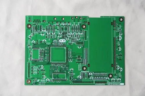
I have been making motherboards for more than two years. I have done the design of Loongson 2F memory and on-board memory particles, and have done the design of Atom N450 memory and on-board memory particles. I want to write something to summarize, and I found that there are already many such articles on the Internet, and now I write a little bit more as a reference supplement. The following content is mainly for the design of DDR2 667 memory.

Signal grouping:
In DDR2 wiring, it is customary to divide the signals into several groups for design, and the signals divided into the same group have related or similar signal characteristics.
Clock group: Differential clock signal, each pair of signals are of the same frequency and phase. ckp0 and ckn0 are a pair.
Data group: For the motherboard 64-bit DDR2 memory, every 8 bits (that is, a byte) of data can be divided into eight groups. Data dq[0:7], data mask dqm0, data strobe differential signal dqsp0 and dqsn0 is a group, and so on. The signals of the same data group should be routed on the same signal layer, and the layers should also be changed together. In order to facilitate the wiring on the same signal layer, the data bits can be exchanged. For example, when the dq2 signal is routed, it is found that if it is routed according to the schematic diagram, it will be interleaved with the dq4, so that the layer has to be changed. We can make the signal go to the same layer by exchanging the data bits. What content is stored in the bit is also what content is read out. The swap will not be affected, but the swap condition must be between 8 bits in the same group.
Address/command group: MA[0:14], BA0, BA1, BA2, RAS, CAS, WE
Control group: Clock enable CKE, chip select CS, and terminal resistance strobe ODT are a group. For the memory module, DIMM0 uses CKE0, CKE1, CS0, CS1, ODT0, ODT1. When designing on-board memory, you can use CKE0, CS0, ODT0 to control 4 16-bit memory chips.
PCB stack:
For a six-layer board, the general stacks are top, GND, singnal2, singnal3, POWER, and bottom. Generally, it is better to use GND as the reference plane for the signal. The impedance of the trace is determined by the width of the trace, the thickness of the copper foil of the trace, the distance from the trace to the reference plane, the thickness of the copper foil of the reference plane and the board dielectric material. The PCB design should comply with the impedance design requirements of the CPU manufacturer to set the stack. Floor. General PCB design software can also calculate impedance. After finding the PCB manufacturer and knowing the material of the sheet dielectric thickness, you can design the stack and line width by yourself. The address/command signal and the control signal can use the 1.8V memory working voltage as the reference plane.
Length control:
For high-frequency signals such as DDR2, the trace length should be calculated to the CPU core, which introduces a concept called package length. The silicon wafer is etched into a CPU core by physical and chemical methods, and then the CPU core is packaged on a small PCB substrate to become our common CPU. The trace length from the pins on that small PCB to the CPU core is called the package length.
The length of the clock to the same rank memory should be controlled within plus or minus 5 mils.
The length of all traces in the same data group should be controlled within the range of plus or minus 20 mils of the data strobe signal DQS. The length can be different between different data groups, but it should be controlled within plus or minus 500 mils of the clock signal.
The address/command group signal length control is not particularly strict. INTEL Atom N450 requires the control of the clock signal within minus 500 mil to plus 1000 mil. That is to say, the difference between the longest and shortest signal can be 1500mil, but it is better to reduce the signal length difference as much as possible when wiring. There is no problem when the signal lengths of these groups are completely equal when wiring, but it takes up a lot of PCB space and takes a lot of time. If the length of the address/command signal exceeds several thousand mils of the clock signal, it needs to be adjusted in the BIOS firmware. The control is within the scope of the CPU requirements. When onboard memory is needed, only the memory SPD needs to be configured.
The control group signal length control requirements are similar to the address/command group signal requirements. When designing, it should be done in accordance with the requirements of the CPU manufacturer. The INTEL Atom N450 requires the clock signal to be controlled within 0mil to plus 1000mil.
Trace spacing:
Generally speaking, the wiring should be routed according to the 3W principle, that is, the line-to-line spacing on the same plane is 3 times the line width. But this is not necessary, the requirement of intel is relatively small. Generally, the spacing of the meandering traces can be 16 to 20 mils, and it can be increased to 30 mils for the clock signal. The distance between the different groups of signals should be appropriately enlarged, which can be more than 20 mils, and the distance between the address/command group and the control group signals can be smaller than 8 mils. The distance between the BGA fan-out areas can be small, and the cables should be routed according to the CPU design requirements after the cables are routed out.
other:
A 20mil line can be used for the VREF trace, and a 0.1uf capacitor should be added to each device.
The VTT trace should be above 135mil, and every four resistors should be connected to a 0.1uf capacitor, and both ends should be connected to a 10uf capacitor.
The above is the introduction of DDR2 wiring in PCB design. Ipcb is also provided to PCB manufacturers and PCB manufacturing technology