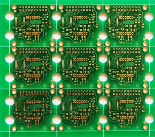
Let me talk about the experience of copper coating, and talk about your views
The so-called copper pour is to use the unused space on the PCB as a reference surface and then fill it with solid copper. These copper areas are also called copper filling. The significance of copper coating is to reduce the impedance of the ground wire and improve the anti-interference ability; reduce the voltage drop and improve the efficiency of the power supply; in addition, it is connected to the ground wire to reduce the loop area. If the PCB board has many grounds, such as SGND, AGND, GND, etc., how to pour copper? My approach is to use the most important "ground" as a reference to pour copper independently according to the position of the PCB board. The digital ground and analog ground are separated to pour copper. At the same time, before pour copper, thicken the corresponding power connections: V5.0V, V3.6V, V3.3V, etc. In this way, multiple deformable structures with different shapes are formed.

There are several problems to be dealt with in copper coating: one is the single-point connection of different grounds, which is connected through 0 ohm resistors or magnetic beads or inductance; the other is copper coating near the crystal oscillator, and the crystal oscillator in the circuit is a high-frequency emission source. It is to coat copper around the crystal oscillator, and then ground the shell of the crystal oscillator separately. The third is the problem of isolated islands (dead zones). If you think it is too big, it will not cost much to define a ground via and add it.
In addition, whether large-area copper pour is better or grid copper pour is better, it is not good to generalize. why? If the copper is covered with a large area, if the wave soldering is used, the board may be uplifted or even blistered. From this point of view, the heat dissipation of the grid is better. Usually it is a multi-purpose grid with high anti-interference requirements for high-frequency circuits, and circuits with large currents in low-frequency circuits are commonly used with complete copper. However, a hero once told me that impedance matching must be used for signals above 1GHz, and the reflective surface must be full copper!
Personal experience: When starting wiring, the ground wire should be treated equally. When routing the wire, the ground wire should be routed well. You cannot rely on adding vias to eliminate the ground pins for the connection after copper pour. This effect is very bad. . Of course, if the grid copper is used, these ground connections will affect the appearance. If you are careful, delete it.
Finally, summarize the benefits of copper coating: improve power efficiency, reduce high-frequency interference, and another is that it looks beautiful!
The above is the introduction of copper plating experience. Ipcb also provides PCB manufacturers and PCB manufacturing technology.