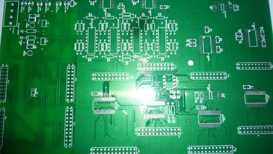
This scheme can be considered when the inter-disturbance can be controlled;
*Ten-layer PCB board: recommended plan 2, 3, available plan 1, 4
Option 3: Expand the respective spacing between 3-4 and 7-8, reduce the spacing between 5-6, the main power supply and its corresponding should be placed on the 6th and 7th layers; preferably the wiring layers S2, S3, S4, followed by S1, S5; this solution It is suitable for occasions where the signal wiring requirements are not much different, taking into account performance and cost; it is recommended for everyone to use; but it is necessary to avoid parallel and long-distance wiring between S2 and S3;
Option 4: EMC effect is excellent, but compared with Option 3, one wiring layer is sacrificed; for key single boards that require low cost, high EMC indicators, and dual power supply layers, this solution is recommended; the wiring layer is preferred S2, S3, for the case of a single power layer, first consider Option 2, and then consider Option 1. Option 1 has obvious cost advantages, but there are too many adjacent wiring, and parallel long lines are difficult to control;
*Twelve-layer board: recommended plan 2, 3, available plan 1, 4, alternate plan 5
Among the above schemes, schemes 2 and 4 have excellent EMC performance, and schemes 1 and 3 have better cost performance;
For single boards with 14 layers and above, due to the diversity of their combinations, they will not be listed here. You can make specific analysis based on the actual situation according to the above arrangement principle.
The above layer arrangement is a general principle and is for reference only. In the specific design process, you can combine the above arrangement principles according to the number of power layers required, the number of wiring layers, the number and proportion of signals required for special wiring, and the division of power and ground. Flexible
Where are the various solutions after the 6-layer board?
The 6th and 8th floors are coming
*Six-layer board, preferred plan 3, available plan 1, alternate plan 2, 4

Scheme Power Ground Signal 1 2 3 4 5 6
1 1 1 4 S1 G S2 S3 P S4
2 1 1 4 S1 S2 G P S3 S4
3 1 2 3 S1 G1 S2 G2 P S3
4 1 2 3 S1 G1 S2 G2 P S3
*Eight-layer board: preferred plan 2, 3, available plan 1
Scheme Power Ground Signal 1 2 3 4 5 6 7 8
1 1 2 5 S1 G1 S2 S3 P S4 G2 S5
2 1 3 4 S1 G1 S2 G2 P S3 G3 S4
3 2 2 4 S1 G1 S2 P1 G2 S3 P2 S4
4 2 2 4 S1 G1 S2 P1 P2 S3 G3 S4
5 2 2 4 S1 G1 P1 S2 S3 G2 P2 S4
EMC problem
You should also pay attention to EMC suppression when laying out the board! ! This is very unsure, distributed capacitance exists at any time! !
How to ground!
PCB design originally has to consider many factors, and different environments need to consider different factors. In addition, I am not a PCB engineer and I am not experienced:)))
Ground division and tandem
Grounding is one of the important means to suppress electromagnetic interference and improve the EMC performance of electronic equipment. Correct grounding can not only improve the product's ability to suppress electromagnetic interference, but also reduce the product's external EMI emission.
The above is the introduction of the solutions that can be considered when the inter-disturbance can be controlled. Ipcb is also provided to PCB manufacturers and PCB manufacturing technology.