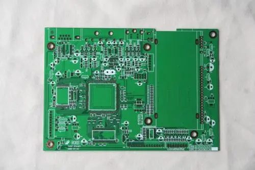
When designing a PCB board, sometimes due to the limitation of the board area or the complicated wiring, it is considered to punch vias on the pads of the SMD components. There have always been two opinions: support and opposition. But in general, based on the author's many years of practical experience, I feel that the way of punching holes on the pads is likely to cause the virtual soldering of the SMD components, so use it with caution as a last resort. The two viewpoints are briefly described as follows.

support:
Generally, the purpose of drilling through holes on the pad is to enhance the overcurrent capability or enhance the heat dissipation. Therefore, the back side is mainly copper to connect to the power or ground. SMD components are rarely placed. In this way, in order to prevent tin leakage during reflow soldering, you can Add green oil to the back of the via, and the problem is solved. This is how the power supply part of the server motherboard I've touched is handled in this way.
be opposed to:
Generally, SMD components can be used in one of the reflow soldering process or the wave soldering process. The wave soldering requires that the pad density should not be too high. Too dense pads can easily cause short-circuit with tin. SMD IC pins are relatively dense. Reflow soldering is used. It is the preferred solution.
Insert files can only use wave soldering.
There are many introductions about wave soldering and reflow soldering on the Internet.
Engineers engaged in PCB design, please understand these production processes before knowing how to design.
There is a Fanout rule in Protel, which prohibits punching vias on the pads.
Traditional craftsmanship prohibits this because the solder will flow into the vias. There are two processes, micro vias and plug holes, which allow the vias to be placed on the pads, but they are very expensive. Please consult the PCB factory.
It is best not to punch through holes in the PAD, which may cause false soldering. Organize the layout, and the location of a small via should still be found.
However, for SMD components, the solder will flow away through the vias during reflow soldering. So use it with caution.