Nothing is best, according to the actual situation

The general stacking order is spss or spps, s is the wiring layer, p is the power layer, and the second layer is preferably the ground layer.
First layer signal
Second layer gnd
Third layer POWER
The fourth floor SIGNAL
Agree with jennry, generally this stackup! But the key to the fundamental principle is to see what kind of board you are and what level you want to achieve. Ha ha!
I agree with the statement on the fourth floor. I think it depends on the actual situation, such as the density of the signal line, the frequency of work, etc.
For general boards, I would like to ask about the ratio of S GS P stacking and S GP S
What is the main difference?
To: I haven't seen stackups like t3322 SGSP, maybe I don't know much about it, haha! This should not be a very good stackup method!
The power and ground are too far away, the plane coupling is not good, and the interference to the signal in the middle is too great! Especially when power transient current, a lot of interference will pass the signal!
When dealing with laminated design, we must first understand the principle of characteristic impedance, the PCB laminated production process and the conditions required by your circuit. The laminated design can be said to be our first procedure in PCB design, and it also affects SI/ PI/EMI and production cost, roughly speaking, first find the minimum feasible process from the circuit characteristics, and then find the corresponding impedance line width of each layer. As for how to configure the P/G layer; refer to the PCB production process and PI impedance And EMI shielding and other issues. When the above considerations have found a balance point, the relevant stack mode and stack thickness are believed to be calculated. If you are interested in learning more, you can search for relevant keywords on the Internet; There are many documents for reference.
Feel free to chat, don't mind too much. I also hope to be helpful. Thanks!
There are two main stacking schemes: SGPS and SPGS.
These two stacked solutions have their own strengths.
From the perspective of EMI, SGPS is better, because most of our parts are placed on the top layer, and the second layer is the ground layer, which has certain advantages in suppressing EMI.
From the perspective of Layout, SPGS is obviously better, because many signal lines require ground reference, and the fourth layer (BOTTOM layer) can be used as the main signal layer, while the fourth layer is very good, and the third layer is a complete ground layer., This is very conducive to wiring.
Generally speaking, if the chip design specification does not explicitly require the second layer to be ground, it is recommended to use the SPGS solution, after all, wiring is the most important.
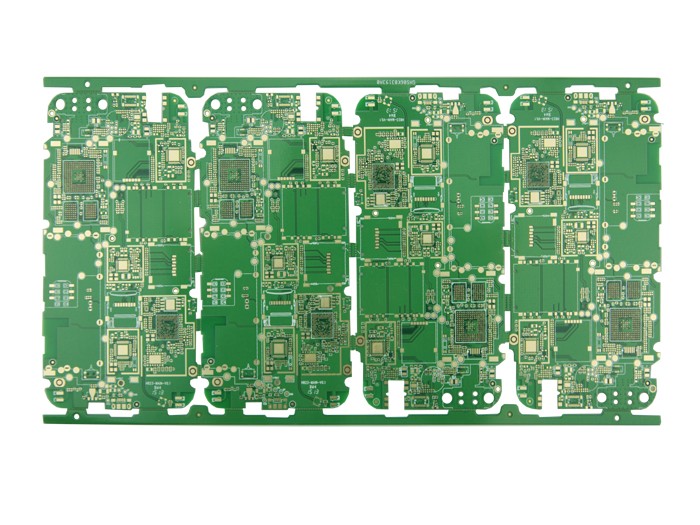
The above is an introduction to the best stacking solution for four-layer PCB boards. Ipcb is also provided to PCB manufacturers and PCB manufacturing technology.