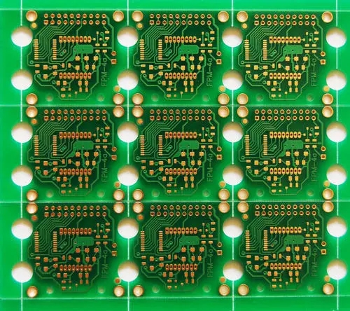
Need to pay attention to those problems in copper plating

1. If the PCB has many grounds, such as SGND, AGND, GND, etc., according to the position of the PCB board, the main "ground" is used as a reference to independently pour copper, digital ground and analog ground. It's not much to say that the copper is applied separately. At the same time, before the copper, first thicken the corresponding power connection: 5.0V, 3.3V, etc., in this way, multiple deformed structures with different shapes are formed.
2. For single-point connections to different grounds, the method is to connect through 0 ohm resistors or magnetic beads or inductance;
3. Copper-clad near the crystal oscillator. The crystal oscillator in the circuit is a high-frequency emission source. The method is to coat the copper around the crystal oscillator, and then ground the shell of the crystal oscillator separately.
4. The island (dead zone) problem, if you think it is too big, it won't cost much to define a ground via and add it in.
5. At the beginning of the wiring, the ground wire should be treated the same. When routing the ground wire, the ground wire should be routed well. You cannot rely on adding vias to eliminate the ground pins for the connection after copper plating. This effect is very bad.
6. It is best not to have sharp corners on the board (<=180 degrees), because from the perspective of electromagnetics, this constitutes a transmitting antenna! For other things, it is only big or small. I recommend using the edge of the arc.
7. Do not apply copper in the open area of the middle layer of the multilayer board. Because it is difficult for you to make this copper "good grounding"
8. The metal inside the device, such as metal radiators, metal reinforcement strips, etc., must be "good grounding".
9. The heat dissipation metal block of the three-terminal regulator must be well grounded. The ground isolation strip near the crystal oscillator must be well grounded. In short: if the grounding problem of the copper on the PCB is dealt with, it is definitely "pros outweigh the disadvantages". It can reduce the return area of the signal line and reduce the electromagnetic interference of the signal to the outside.
The above is an introduction to the issues that need to be paid attention to in copper deposition. Ipcb is also provided to PCB manufacturers and PCB manufacturing technology.