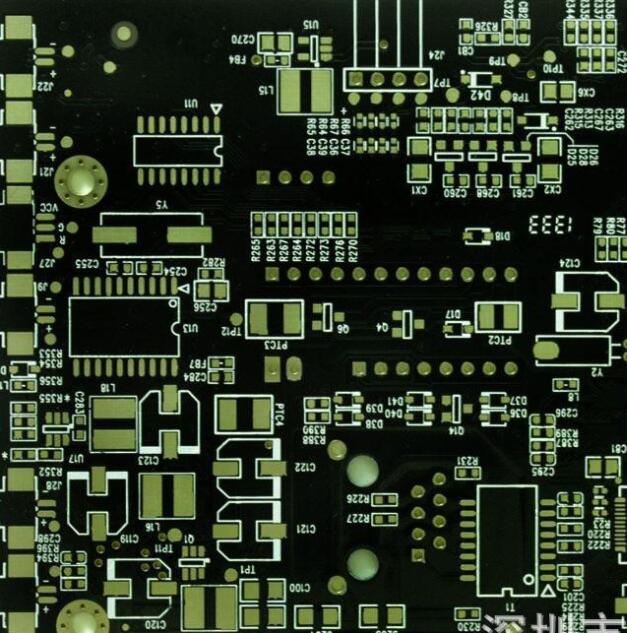
Now the electronic product development is more and more miniaturized, the board is smaller and smaller, the more delicate, for the general digital circuit board size is determined by the chip and power supply device, the performance is basically stable, strong anti-interference ability, at the same time the signal frequency is relatively low.
However, for the PCB of hf signal and RF circuit board,PCB layout is more exquisite, PCB wiring will affect the final signal demodulation and reception, affecting the stability and reliability of the product. Therefore, PCB design for high frequency signal wiring requirements. At this time, the resistance and capacitance parameters caused by PCB wiring need to be taken into account, which cannot be ignored.
The resistance values of different widths are different at different temperatures. For example, at 25 degree Celsius, if they are covered with 1Oz thick copper, the resistance values of DIFFERENT PCB transmission line lengths MIL have the following curve relationship.
When PCB of the same length goes offline, the wider the line width, the smaller the resistance value.
At 125 degree Celsius, for 1oz copper covered area, PCB transmission line resistance is related to length and width as follows:

By comparison, the higher the temperature is, the resistance will increase when the line length and line width are the same. As shown in the figure, the resistance value of the 20mil by 5mil 1Oz copper-coated resistor increases by 1m ω.
Therefore, the design needs to consider the application of ambient temperature and flow capacity, design appropriate line width and line length.
In PCB design, the capacitance is affected by parallel wiring. The calculation formula of inter-board capacitance of parallel wiring is as follows:
K = Permittivity of free space vacuum Permittivity, k = 8.854 ∙10-3 pF/mm in metric units and 2.247 ∙10-4 pF/mil in Imperial units.
ℓ is the length, which is mm in metric and mil in British.
W is width, mm in metric and Mil in British.
H = separation between planes (mm in metric and MIL in British)
εr = PCB relative dielectric constant, for PCB board FR-4, ε R ≈ 4.5.