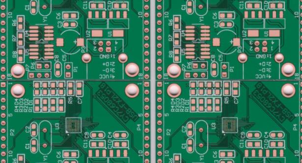
What problems should be paid attention to when PCB proofing and patching?
The purpose of PCB circuit board proofing is to detect whether the circuit board has problems and whether it can have all the functions before mass production, which avoids the scrap and waste of costs caused by mass production if there are any problems. Therefore, PCB proofing patch Is very important, let's take a look at the precautions below.
SMT
First, the requirements of the engineer for the PCB board proofing and patch
1. First, we must understand the specific situation, so as to choose the most reasonable number of PCB proofing patches, no more and no less, until it is suitable, so that the cost can be greatly reduced.
2. Check all the device packages, and don’t end up with proofing failures due to package errors.
3. Do a comprehensive electrical inspection of the PCB circuit board to improve the electrical performance of the circuit board and improve the safety performance.
4. The layout of the signal integrity should be planned well, and no noise should appear, so that the stability of the circuit board will not be affected.
Second, PCB circuit board proofing and patch requirements for manufacturers
1. Do a good job in the certification and comprehensive inspection of PCB files, and there should be no data problems.
2. The industrial approval must be comprehensive and standardized, and the process configuration must be perfect.

3. Conduct comprehensive and in-depth communication with customers to further understand customer needs and precautions to avoid some mistakes.
Three, what are the precautions in the process of proofing and patching PCB circuit boards
1. Do a good job in the layout and wiring of each component
If you want to ensure the life and stability of the product, and maintain the electromagnetic compatibility of the product, you must do a good job in the layout and wiring of the components. This is the most important point. The placement order of the components must be correct. You can first place the components in a fixed position related to the structure, and then place other components in the order from largest to smallest. In the layout, the heat dissipation of the components should also be considered. For components that generate heat, they should be placed separately and cannot be concentrated together, which is not conducive to heat dissipation and affects the service life.
PCB board
2. Further improve other factors
After the PCB circuit board is wired, it is necessary to make some adjustments to the text, individual components, wiring, and copper. The purpose of this is to facilitate production, debugging, and maintenance.
3. The simulation function PCB circuit board proofing is more realistic
In order to improve the accuracy of PCB circuit board proofing, the simulation functionPCB circuit board can be used for proofing, which can ensure the effect, especially for high-frequency digital circuits, which can find and solve problems in advance, thus reducing the workload of later debugging., Greatly improve work efficiency.
SMT patch
In short, when doing PCB proofing and patching, it is best to find a more professional company, which must have many years of PCB circuit board production, design, and proofing experience to ensure the correctness and high efficiency of the proofing work.