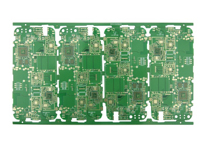
Now PCB has developed to a new stage. The introduction of new technologies such as high-density interconnect (HDI) PCB and IC substrate (ICS) has made the entire production process from manual to fully automated. With the further development of manufacturing technology, the process becomes more and more complex, and defect inspection becomes more and more important and more difficult. These fatal defects may lead to the scrapping of the entire PCB board. For the PCB manufacturing industry, opportunities to use artificial intelligence (AI) and optimize the production process and ultimately optimize the entire PCB manufacturing process are emerging.
PCB manufacturing usually relies on experts who have accumulated knowledge for many years. These experts know and understand each step of the manufacturing process very well. They understand how to use their knowledge to optimize production and increase yield. Human constraints (including misoperation and fatigue) hinder efficiency growth. Operator errors or misidentification of PCB defects ("false alarms") may affect yield due to overprocessing, and even damage the PCB itself. By integrating AI into the manufacturing process, machines can add value by taking over certain "learning" tasks, while human experts continue to take on more complex tasks that require thinking and interaction while optimizing and "training." Artificial intelligence system. The combination of humans and artificial intelligence improves overall efficiency and operations, and is the biggest opportunity for AI systems.
Artificial Intelligence and Industry 4.0
The final trend of PCB development is to have a factory that fully integrates the Industry 4.0 system, which uses AI technology at the global and manufacturing system level. The "global" level includes all systems in the factory, not just a single manufacturing system.

Industry 4.0 provides an automation and data exchange infrastructure that can realize real-time production analysis, two-way communication and data sharing, traceability, and on-demand data analysis. In any particular factory, AI can use data obtained from various manufacturing systems and machines to improve processes. These data are collected through Industry 4.0 mechanisms (such as traceability, two-way communication). The factory benefits because AI analyzes a large amount of system-wide data to optimize factory settings and achieve the highest level of productivity and yield. Artificial intelligence analysis and self-learning are in progress and are carried out through artificial neural networks. Within a few years, it will eliminate manual operator intervention and lead to the establishment of fully automated factories.
This new PCB manufacturing model requires full connectivity of all factory systems and AI as a monitoring and decision-making mechanism. Currently, there are proprietary and technical challenges that limit the complete automation of PCB factories, but AI has been added to a single system as much as possible, such as automated optical inspection (AOI) solutions. The advantages of moving production facilities to a global AI model include the ability to more reliably notify PCB defects-"real defects", and a feedback mechanism that can identify the root cause of the problem, and then automatically modify the factory process to eliminate related problems and defects .
A subset of AI, including machine learning and deep learning, will enable PCB factories to move towards full automation. The algorithms used by machine learning enable computers to use data and the examples it has gone through and learned from it to improve the performance of tasks without the need for explicit programming. As far as PCB manufacturing is concerned, machine learning can increase production, improve manufacturing operations and processes, and reduce manual operations, while helping to promote more effective processing of factory assets, inventory, and supply chains.
Deep learning promotes AI to a more complex level, which is beneficial at the global factory system level. Deep learning is inspired by human brain neurons, the ability of multi-layer artificial neural networks to learn, understand and infer. In a PCB factory, the software system can effectively collect data and learn from complex representations of patterns and contexts. Then, learning will form the basis for automatic process improvement in PCB manufacturing.
The implementation of machine learning and deep learning provides PCB manufacturers with capabilities beyond human understanding; artificial intelligence systems discover new optimization opportunities by digging deeper in places that people are unwilling to explore. The AI expert system is very efficient. By using more and more complex parameters to monitor the factory system on a global scale, it reduces the number of human experts required and improves efficiency and best practices.
Using Industry 4.0 sensors (sensors that can send data from devices) and systems, in the entire PCB manufacturing process, from simple reading and writing functions to advanced tracking of process parameters, up to the smallest PCB unit, it can be created on a global scale data. Process parameters can include etching, resist development and even the concentration of chemical materials in the manufacturing process. Use deep learning to analyze these types of data to inform optimized manufacturing methods and parameters, identify patterns, and make informed decisions about changes required in the process. All of these can be performed 24 hours a day, 7 days a week, 24 hours a day, 7 days a week.
System-level AI
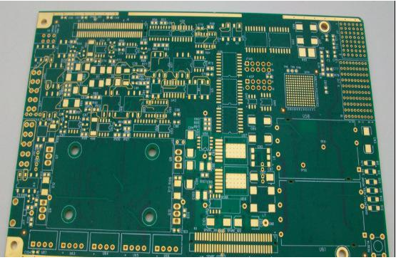
At the system level, such as in the AOI process, the implementation of AI in the PCB manufacturing workshop has a considerable impact on productivity and yield. In this case, machine learning greatly reduces human error when detecting PCB defects. Examples of PCB defects include short circuits and open circuits, even excessive copper. Automated inspection can detect very small defects. These defects may not be found by manual inspection, or they may be missed due to human error. This is the natural result of repeated work.
By performing machine learning on the AOI system, such false alarms and repairs can be greatly reduced. Fewer false alarms means less processing of the PCB board, which will also increase efficiency. In addition, AI provides consistent (dynamically improved) defect classification without the inherent limitations of operators, thereby providing more reliable results and reducing verification time. According to Orbotech's internal research, it has been found that the AI in the AOI system can reduce false alarms by up to 90%. AOI is unique in that the system can collect more data than any other manufacturing solution, which makes it very suitable as the first step in AI implementation. At the same time, the AOI room is the most labor-intensive area of the PCB factory. Therefore, the use of AI in its process will bring the greatest benefits. For PCB manufacturers, all of this means that millions of defects can be identified and classified more accurately, which may increase yields and reduce costs.
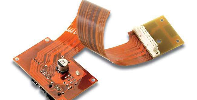
Although the development of AI is developing rapidly across the industry, the challenges in PCB manufacturing are growing at the same rate, or even faster. For flexible materials and reduced trace geometry, there are two difficult areas for defect detection. Next-generation composite materials, such as liquid crystal polyamide (LCP) and modified polyamide (MPI), present new challenges for manufacturers, including image acquisition, processing, deformation, and thinner lines. For example, the more advanced the materials used for flexible PCBs, the more defects are identified, which leads to more false alarms. The manufacturer's purpose in using this complex material is to minimize the handling of panels in the process of determining false alarms. Therefore, Flex PCB is a product type that will likely benefit greatly from AI implementation, because the system will learn to manufacture within stricter parameters. PCBs for 5G are another highly demanding one, and it is possible to benefit greatly from the expertise supported by artificial intelligence. HDI PCBs required for 5G applications require finer line widths, straight sidewall geometries and strict parameters. This makes defect detection more difficult than ever, and it will be extremely challenging for human experts to effectively complete defect detection.
Considering these and other unknown PCB manufacturing challenges, artificial intelligence-driven factories will become the key to future production. To realize the development of AI applications on a global scale, it takes more time to realize PCB manufacturing, but it is clear that the realization of system-level AI has arrived, laying the foundation for the future of fully automated PCB factories.