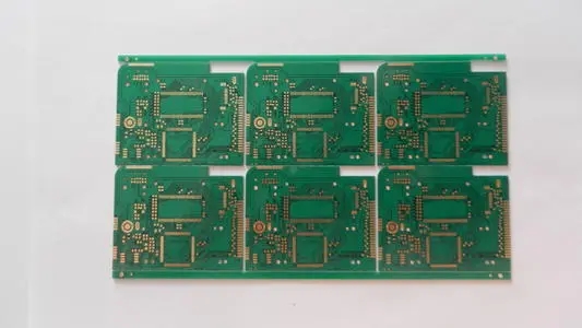
When the customer does not provide the drilling file, in addition to the hole diameter hole position can be converted into a drilling hole, it can also be converted into a drilling file with the line PAD. When it is not easy to make a Flash when the aperture and hole position symbols intersect, or when the number of holes is not given (a general guide to through holes), the above method is better. First copy all the PADs on the circuit to an empty layer, make Flash according to the aperture size, and then delete the redundant paste PADs and convert them into drilling files.

2. When the solder mask and circuit PAD match mostly does not meet the process capability, all circuit PADs can be copied to an empty layer, use this layer and the solder mask layer to delete the redundant circuit PAD, and then enlarge this layer as a whole by 0.2mm (Enlarge or reduce the overall size: Utilities-->Over/Under), and finally copy the soldering strip or block (on the large copper) of the solder mask. Use this method to do the solder mask must be carefully compared with the original solder mask to prevent more or less solder mask.
3. When the material is covered by a large area of copper foil, the distance between the circuit or PAD and the copper skin is not within the production requirements, and the appearance size is large, (such as Guangshang) can use the following methods to quickly repair the circuit or PAD and copper The spacing of the skins. First copy all the PADs on the circuit layer (this layer is the first layer) to an empty layer,
After the PAD is deleted, enlarge the remaining PAD as the subtractive circuit layer (ie the second layer), then copy the first layer to an empty layer, and delete the large copper skin as the third layer. The layering method is: the first layer (additional layer), the second layer (subtractive layer), and the third layer (additional layer). Generally speaking, in order to reduce the amount of data, we can keep the first layer only large
Copper skin. If the distance between the solder mask and the large copper skin is not enough, you can copy the enlarged solder mask (meeting the process capability) to an empty layer, delete the solder mask corresponding to the large copper skin, and enlarge the remaining solder mask as Second floor.
Note: After completing the PCB circuit with this method, you must use the command to convert a composite layer of Utilities-->Convert Composite into a layer, and then use the Anglysis-->Compare Layers command to carefully perform this layer and the original Check.
4. When the text layer of some data has many text boxes, and the distance between the text box and the line PAD does not meet the process capability, the following method can be used for reference: first use the Edit-->Move Vtx/Seg command to pull any type of text box After reaching the specification range, it will be made into Flash, and then other text boxes of the same type can be made into the same Flash. But it should be noted that after making the Flash, it must be broken up to prevent the D code from rotating when the data is opened.
The above is an introduction to the exchange of CAM350 skills. Ipcb is also provided to PCB manufacturers and PCB manufacturing technology.