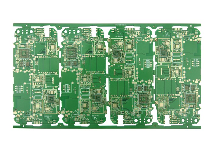
Copper is a strong conductor with a high melting point, but you should still try to keep it cold. Here, you need to adjust the width of the wire to keep the temperature within a certain range. However, this is where you need to consider the current flowing in a given line. When using power rails, high-voltage assemblies, and other heat-sensitive parts of the PCB board, the PCB wiring width can be determined by its relationship to the ammeter to determine the wiring width to be used in the layout.

One problem with most tables is that they do not solve the problem of controlled impedance routing. You have determined the size of the wiring to control the impedance, it is difficult to determine the temperature rise just by looking at the table, and you must use a calculator. However, an alternative method is to use the IPC2152 Normogram to check whether the current-temperature relationship is within the operating range of the controlled impedance curve.
In my day job, I find myself spending a lot of time browsing EE forums. A problem that often arises during PCB design and wiring is determining the recommended wiring width to keep the temperature of the device within a certain range of a given current value, and vice versa. Although copper has a high melting point and can withstand high temperatures, ideally you should keep the temperature rise on the board to no more than 10°C. Allowing PCB wiring to reach very high temperatures increases the ambient temperature seen by the component, which places a greater burden on active cooling measures.
The IPC2152 standard is the place where sizing thread and through-hole start. The formulas specified in these standards are simple for calculating current limits for a given temperature rise, although they do not take into account controlled impedance wiring. Having said that, using a PCB trace width and ammeter is a good starting point when determining PCB trace width/cross-sectional area. This allows you to effectively determine the upper limit of allowable current in wiring, which can then be used to resize the wiring for controlled impedance wiring.
When the temperature rise on the board operating at high current reaches very large values, the electrical properties of the substrate will show corresponding changes at high temperature. The electrical and mechanical properties of the substrate vary with temperature, and the substrate will discolor and weaken if it is run at high temperatures for long periods of time. This is one of the reasons I know designers who size their wiring to keep the temperature rise within 10°C. Another reason for doing this is to accommodate a wide range of ambient temperatures, rather than considering a specific operating temperature.
The PCB trace width versus current chart below shows the trace width and the corresponding number of current values that will limit the temperature rise to 10°C by 1oz/sq. Feet of copper. This should give you an idea of how to resize the wiring in the PCB.
Different wiring thickness/copper weight. Trace thickness should be calculated according to the weight of copper on the plate. We only included the standard 1 ounce/sf. Values above feet. However, circuit boards intended to operate at high currents typically require heavier copper to accommodate higher temperature rises. No impedance data. If controlled impedance routing is required, verify that the calculated routing dimensions meet the limits specified above.
Substitute substrate. The data above is compiled for FR4 and will cover a large number of PCBS already in production. However, applications may require aluminum core PCBS, ceramic substrates or high-speed laminates. If you use a substrate with high thermal conductivity, the wiring temperature will decrease as heat is taken away from the warm wiring. For first-order approximations, the temperature rise will be scaled by the ratio of the thermal conductivity of the required substrate to the thermal conductivity of FR4.
If different copper weights are to be used, verify the controlled impedance wiring dimensions for temperature rise and current, and then use the IPC2152 standard row diagram. This is a good way to determine the size of the conductor for specific current and temperature rises. In addition, if you have selected the line width, you can determine the current that will cause a particular temperature increase. This is shown in the two examples in the columnar diagram below. The red arrow shows how to determine the desired wiring width, copper weight (i.e. wiring cross-sectional area) and temperature rise current. In this example, first select the conductor width (140 mil), and then draw the red arrow horizontally to the desired copper weight (1 ounce/square foot). We then trace vertically to the desired temperature rise (10°C) and then back to the Y-axis to find the corresponding current limit.
The orange arrow moves in the other direction. We start with the required current (1A) and track horizontally to the required temperature rise (30°C). Then, we track vertically down to determine the tracking size. In this example, suppose we specify 0.5oz/sq. Feet of copper. So once we trace back to this line, we trace horizontally back to the Y-axis to find what? 40 mils of conductor width. Let's say the copper we want to use weighs 1oz/sq. The ft. ; In this case, we find that the required wiring width is 20 mils.