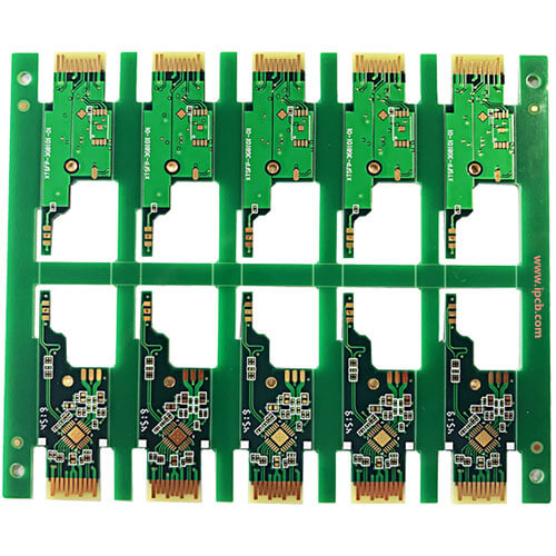
To do high-speed PCB design, you must first understand the following basic concepts, which are the foundation.

1. What is electromagnetic interference (EMI) and electromagnetic compatibility (EMC)?
(Electromagnetic Interference), there are two kinds of conducted interference and radiated interference. Conducted interference refers to the coupling (interference) of signals on one electrical network to another electrical network through a conductive medium. Radiated interference refers to the interference source coupling (interference) its signal to another electrical network through space. In high-speed PCB and system design, high-frequency signal lines, integrated circuit pins, various connectors, etc. may become radiation interference sources with antenna characteristics, which can emit electromagnetic waves and affect other systems or other subsystems in the system. normal work.
Since the emergence of noise reduction technology in electronic systems in the mid-1970s, it is mainly due to the US Federal Communications Commission in 1990 and the European Union in 1992 that proposed regulations on commercial digital products. These regulations require companies to ensure that their products comply with strict magnetic susceptibility. And launch guidelines. Products that comply with these regulations are called EMC (Electromagnetic Compatibility).
2.What is signal integrity?
Signal integrity refers to the quality of the signal on the signal line. A signal with good signal integrity means that it has the value of the voltage level that must be reached when it is needed. Poor signal integrity is not caused by a single factor, but by multiple factors in board-level design. The main signal integrity problems include reflection, oscillation, ground bounce, crosstalk, etc.
Common signal integrity problems and solutions
problem
Possible Causes
Solution
Other solutions
Overshoot
Terminal impedance mismatch
Terminal termination
Use a drive source with a slow rise time
The DC voltage level is not good
Online load is too large
Replace DC load with AC load
Terminate at the receiving end, rewire or check the ground plane
Excessive crosstalk
Too much coupling between lines
Use a send driver with a slow rise time
Use a drive source that can provide a larger drive current
Too much time delay
Transmission line distance is too long
Replace or renew the line, check the serial termination
Use the driving source of impedance matching, change the wiring strategy
oscillation
Impedance mismatch
Connect the damping resistor in series when sending off
3.What is reflection?
The reflection is the echo on the transmission line. Part of the signal power (voltage and current) is transmitted to the line and reaches the load, but part is reflected. If the source end and the load end have the same impedance, reflection will not occur.
The impedance mismatch between the source and the load will cause reflections on the line, and the load will reflect part of the voltage back to the source. If the load impedance is less than the source impedance, the reflected voltage is negative. On the contrary, if the load impedance is greater than the source impedance, the reflected voltage is positive. Variations in factors such as wiring geometry, incorrect wire termination, transmission through connectors, and discontinuities in the power plane can all cause such reflections.
4. What is crosstalk?
Crosstalk is the coupling between two signal lines, and the mutual inductance and mutual capacitance between the signal lines cause noise on the line. Capacitive coupling induces coupling current, and inductive coupling induces coupling voltage. The parameters of the PCB layer, the signal line spacing, the electrical characteristics of the driving end and the receiving end, and the line termination method all have a certain impact on the crosstalk.
5. What is overshoot and undershoot?
Overshoot is the first peak or valley that exceeds the set voltage-for rising edges it refers to the highest voltage and for falling edges it refers to the lowest voltage. Undershoot refers to the next valley or peak. Excessive overshoot can cause the protection diode to work, leading to premature failure. Excessive undershoot can cause false clock or data errors (misoperation).
6. What is ringing and rounding?
The phenomenon of oscillation is repeated overshoot and undershoot. Signal oscillation and surrounding oscillation are caused by excessive inductance and capacitance on the line. The oscillation belongs to the under-damped state and the surrounding oscillation belongs to the over-damped state. Signal integrity problems usually occur in periodic signals, such as clocks. Oscillation and surround oscillation are caused by many factors like reflection. Oscillation can be reduced by proper termination, but it is impossible to completely eliminate it.
7. What are ground plane bounce noise and return noise?
When there is a large current surge in the circuit, it will cause ground plane bounce noise (referred to as ground bounce). For example, when a large number of chip outputs are turned on at the same time, a large transient current will flow through the power plane of the chip and the board., The inductance and resistance of the chip package and the power plane will cause power noise, which will produce voltage fluctuations and changes on the real ground plane (0V). This noise will affect the actions of other components. The increase of load capacitance, the decrease of load resistance, the increase of ground inductance, and the increase of the number of switching devices at the same time will all lead to the increase of ground bounce.
Due to the division of the ground plane (including power and ground), for example, the ground plane is divided into digital ground, analog ground, shielding ground, etc., when the digital signal goes to the analog ground area, ground plane return noise will be generated. Similarly, the power layer may also be divided into 2.5V, 3.3V, 5V, etc. Therefore, in the multi-voltage PCB design, the bounce noise and return noise of the ground plane need special attention.
8. What is the difference between time domain and frequency domain?
The time domain is the process of voltage or current changes based on time, which can be observed with an oscilloscope. It is usually used to find out the delays, skew, overshoot, undershoot, and settling times from pin to pin.
The frequency domain is the process of voltage or current changes based on frequency, which can be observed with a spectrum analyzer. It is commonly used for comparison between waveforms and FCC and other EMI control limits.
9. What is impedance?
Impedance is the ratio of the input voltage to the input current on the transmission line (Z0=V/I). When a source sends a signal to the line, it will prevent it from driving until 2*TD, the source does not see its change, where TD is the line delay (delay).
10. What is settling time?
The settling time is the time required for an oscillating signal to stabilize to a specified final value.
11.What is the pin-to-pin delay (delay)?
The pin-to-pin delay refers to the time between the change of the state of the driver and the change of the state of the receiver. These changes usually occur at 50% of a given voltage. The minimum delay occurs when the output first crosses the given threshold (threshold), and the maximum delay occurs when the output last crosses the voltage threshold (threshold). Measure all of these Condition.
12.What is skew?
The signal offset is the time offset between reaching different receivers for the same network. The offset is also used for the time deviation of the clock and data arrival on the logic gate.
13. What is slew rate?
Slew rate is the slope of the edge (the rate of time change in the voltage of a signal). The technical specification of I/O (such as PCI) is between two voltages. This is the slew rate, which can be measured.
14. What is a quiescent line?
It does not switch during the current clock cycle. It is also called "stuck-at" line or static line. Crosstalk (Crosstalk) can cause a static line to switch within a clock cycle.
15.What is false clocking?
Fake clock means that the clock changes state unconsciously (sometimes between VIL or VIH) when it crosses the threshold. It is usually caused by excessive undershoot or crosstalk.