Wiring direction: From the perspective of the soldering surface, the arrangement of the components should be as consistent as possible with the schematic diagram. The wiring direction is best to be consistent with the wiring direction of the circuit diagram. Because various parameters are usually tested on the soldering surface during the production process, so This is convenient for inspection, debugging and maintenance during production (Note: It refers to the premise that the circuit performance and the installation and panel layout requirements of the whole machine are met).

2. The arrangement and distribution of the components should be reasonable and even, and strive to be neat, beautiful, and strict in structure.
3. Resistor and diode placement methods: there are two types: horizontal placement and vertical placement:
(1) Horizontal placement: When the number of circuit components is small and the size of the PCB circuit board is large, it is generally better to use horizontal placement; for resistors below 1/4W, the distance between the two pads is general Take 4/10 inches, when the 1/2W resistor is placed flat, the distance between the two pads is generally 5/10 inches; when the diode is placed flat, 1N400X series rectifier tubes, generally take 3/10 inches; 1N540X series rectifier tubes, generally Take 4 to 5/10 inches.
(2) Vertical installation: When there are a large number of circuit components and the size of the circuit board is not large, the vertical installation is generally adopted, and the distance between the two pads is generally 1 to 2/10 inches in the vertical installation.
4. Potentiometer: the placement principle of IC holder
(1) Potentiometer: It is used in the regulator to adjust the output voltage, so the PCB design potentiometer should be fully adjusted clockwise when the output voltage rises, and the output voltage of the counterclockwise regulator decreases when the output voltage is reduced; in the adjustable constant current charger The middle potentiometer is used to adjust the size of the charging current. When the potentiometer is designed, the current will increase when the potentiometer is fully adjusted clockwise. The potentiometer should be placed on the position of the unit to meet the requirements of the whole machine structure installation and panel layout, so it should be placed on the edge of the board as much as possible, with the rotating handle facing outward.
(2) IC holder: When designing the printed board diagram, when using the IC holder, be sure to pay special attention to whether the orientation of the positioning slot on the IC holder is correct, and pay attention to whether each IC pin is correct, for example, the first pin can only be used. It is located at the lower right corner or upper left corner of the IC socket, and is close to the positioning groove (viewed from the welding surface).
5. Arrangement of in and out terminals
(1) The distance between the two associated lead ends should not be too large, generally about 2 to 3/10 inches is more appropriate.
(2) The inlet and outlet ends should be concentrated on one or two sides as much as possible, and should not be too discrete.
6. Pay attention to the pin arrangement sequence when designing the wiring diagram, and the component pin spacing should be reasonable.
7. Under the premise of ensuring the performance requirements of the circuit, the design should strive for reasonable wiring, use less external jumpers, and route the wires according to certain smooth charging requirements, and strive to be intuitive, easy to install, height and overhaul.
8. When designing the wiring diagram, the wiring should be as few as possible to bend, and the lines should be simple and clear.
9. The width of the wiring strips and the spacing of the lines should be moderate, and the spacing between the two pads of the capacitor should be as consistent as possible with the spacing of the capacitor lead pins;
10. The design should be carried out in a certain order, for example, it can be carried out in the order from left to right and top to bottom
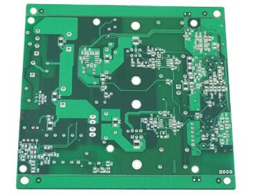
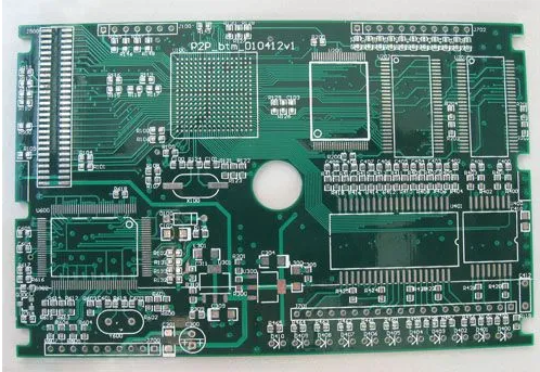
The above is about the following introductions that should be paid attention to in the design of printed board diagrams. Ipcb is also provided to PCB manufacturers and PCB manufacturing technology.